Service hotline
+86 0755-83044319

release time:2024-03-13Author source:SlkorBrowse:17163
In the structure of the power MOSFET, as shown in Figure 1, there is a parasitic capacity.
In terms of the structure of the power MOSFET, as shown in Figure 1, there is a parasitic capacitance. The G (gate) terminal of the MOSFET is insulated from other electrodes by an oxide film, and a PN junction is formed between the DS (drain, source) to form a built-in diode structure. Cgs, Cgd capacity is determined by the capacitance of the oxide film, and Cds is determined by the junction capacity of the built-in diode.
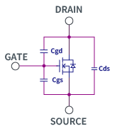
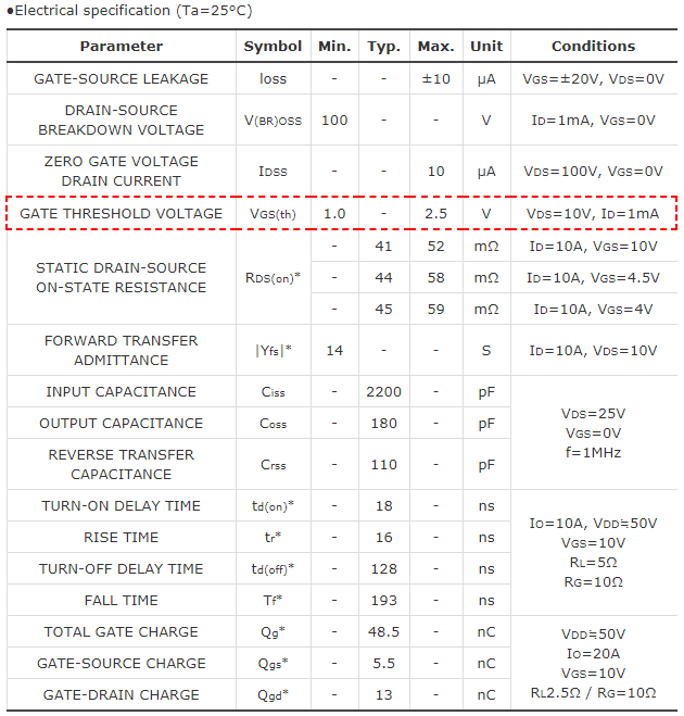
Generally speaking, the three types of Ciss/Coss/Crss in Table 1 are recorded in the MOSFET specification.
| Mark | Formula | Meaning |
| Ciss | Cgs+Cgd | Input capacity |
| Coss | Cds+Cgd | Output capacity |
| Crss | Cgd | Feedback capacity |
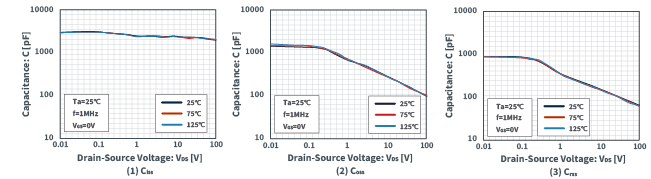
As shown in Fig. 2, the capacitance characteristics depend on the voltage VDS between DS (drain and source). The larger the VDS, the smaller the capacity value.
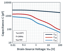
The actual measurement examples are shown in Figures (1) ~ (3)
There is little difference in the temperature dependence of the capacity characteristics.
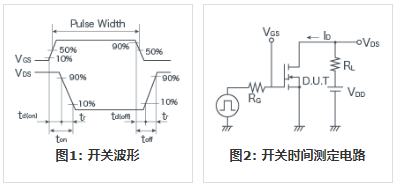
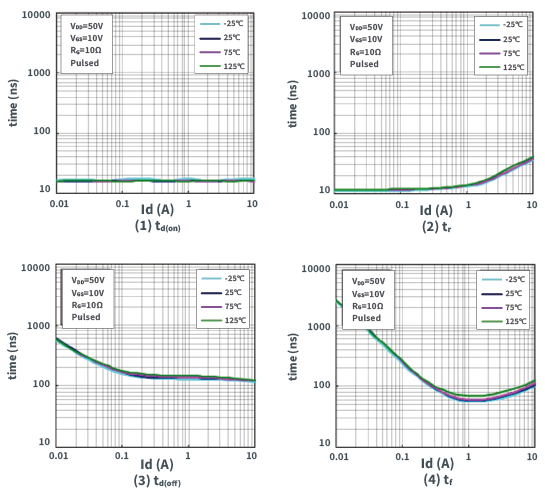
After the gate voltage is ON/OFF, the MOSFET is ON/OFF. This delay time is the switching time. The switching time is as shown in Table 1. Generally speaking, td(on)/tr/td(off)/tf are recorded in the specification.
Slkor determines the typ. value of the specification based on the measured value of the circuit in Figure 2.
The measured examples are shown in Figure 3(1)~(4).
The switching time increases slightly as the temperature rises, but it increases by about 10% when the temperature rises to 100°C, and there is almost no temperature dependence of the switching characteristics.
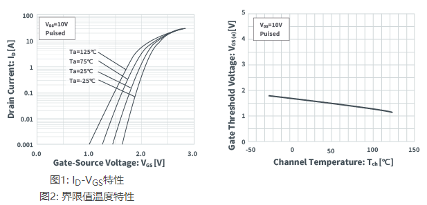
When the MOSFET is turned on, the voltage required between GS (gate, source) is called VGS(th) (threshold value).
That is, when the voltage above the limit value is input, the MOSFET is turned on.
So how much A current can the MOSFET pass through when it is in the on state? For each component, it is recorded in the electrical characteristics column of the specification sheet.
Table 1 is an example of the electrical characteristics column of the specification. In this case, when the input VDS=10V, the gate threshold voltage ID(th) required to pass 1mA current through ID is 1.0V to 2.5V.
Figures 1 and 2 show the actual measurement examples of ID-VGS characteristics and threshold temperature characteristics.
As shown in Figure 1, in order to pass most of the current, a relatively large gate voltage is required.
The models listed in Table 1 have a limit value of 2.5V or less in the specifications, but they are 4V driven products.
When using, please input the gate voltage to make it turn on sufficiently.
As shown in Figure 2, the limit value decreases with temperature.
By observing the threshold voltage change, the channel temperature of the element can be calculated.


Site Map | 萨科微 | 金航标 | Slkor | Kinghelm
RU | FR | DE | IT | ES | PT | JA | KO | AR | TR | TH | MS | VI | MG | FA | ZH-TW | HR | BG | SD| GD | SN | SM | PS | LB | KY | KU | HAW | CO | AM | UZ | TG | SU | ST | ML | KK | NY | ZU | YO | TE | TA | SO| PA| NE | MN | MI | LA | LO | KM | KN
| JW | IG | HMN | HA | EO | CEB | BS | BN | UR | HT | KA | EU | AZ | HY | YI |MK | IS | BE | CY | GA | SW | SV | AF | FA | TR | TH | MT | HU | GL | ET | NL | DA | CS | FI | EL | HI | NO | PL | RO | CA | TL | IW | LV | ID | LT | SR | SQ | SL | UK
Copyright ©2015-2025 Shenzhen Slkor Micro Semicon Co., Ltd
