Today, foundries are living very comfortably, and this state will continue, at least until 2025.
This week, IC Insights released the latest market research report. It is expected that the total sales of the foundry market in 2021 will exceed the US$100 billion mark for the first time, reaching US$107.2 billion, an increase of 23%, compared with 2017. comparable to record growth rates (see Figure 1).
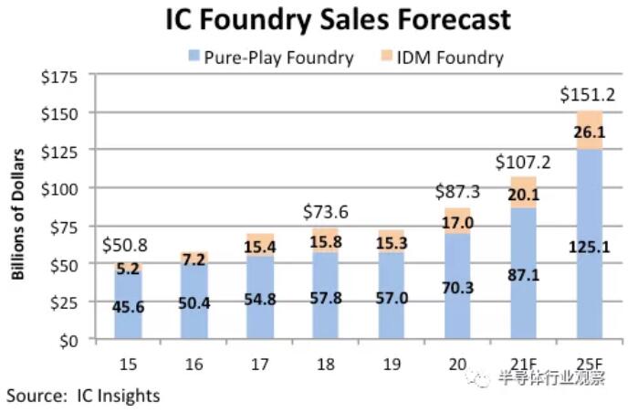 Figure 1
   ; The global foundry market is expected to grow at an average annual growth rate of 11.6% by 2025, with total sales of the era factories reaching US$151.2 billion.
The pure-play foundry market is expected to grow strongly by 24% this year to $87.1 billion, surpassing 23% in 2020. The pure-play foundry market will grow to $125.1 billion by 2025, with a 5-year (2020-2025) CAGR of 12.2%, accounting for 82.7% of total foundry sales in 2025, while 2021 81.2% year-on-year. [敏感词], UMC and several specialty foundries expect healthy sales growth this year. These suppliers are also investing heavily in new capacity to support the expected demand for foundry capacity during the forecast period.
Samsung's external sales, mainly driven by customers such as Qualcomm, account for the majority of the IDM foundry market. IC Insights expects the IDM foundry market to grow 18 percent this year to $20.1 billion. The IDM foundry market is expected to grow to $26.1 billion by 2025, growing at a 5-year CAGR of 9.0%.
Whether it is a wafer foundry or IDM, starting from the second half of 2020, it has entered a mode of crazy production expansion, and 12 inches and 8 inches go hand in hand. With the decline of the inch factory, the market demand is showing an overall strong state.
Globally, the representatives of pure wafer foundries are [敏感词], UMC, GF and SMIC, while the representative companies of IDM in foundry business are Samsung and Intel. Take a look at these performances and actions below.
[敏感词]
[敏感词] announced that its capital expenditure in 2021 will increase from the previously estimated US$25-28 billion to US$30 billion, of which more than 80% will be used for advanced process investment, and 7nm, 5nm, 3nm, 2nm process production lines are all used 12-inch wafer.
Not long ago, [敏感词] also announced a three-year investment of US$100 billion to expand the wafer fab, and confirmed that it would invest US$2.887 billion to expand the 28nm process capacity of the Nanjing plant, increasing the output of 40,000 wafers per month. in the production of automotive chips.
[敏感词] pointed out that at present, the wafer fabs in [敏感词] have no clean room space, and only the Nanjing fab has ready space available, which can directly set up production lines, which is conducive to the rapid formation of production capacity. According to the plan, the 28nm process capacity of [敏感词]'s Nanjing plant will be mass-produced in the second half of 2022, and the full-load capacity target of 40,000 wafers/month will be reached in mid-2023. At present, [敏感词]'s Nanjing plant mainly produces 16nm chips, with a monthly production capacity of about 20,000 wafers.
For [敏感词] to maintain its leadership in 5nm and more advanced processes, EUV lithography machines are an important part. In recent years, the company has continued to purchase EUV equipment to maintain its advanced process capacity advantage. [敏感词] held a technology forum a few days ago, pointing out that the cumulative installed capacity of its EUV equipment will account for 50% of the global total by 2020. By 2020, wafers produced by [敏感词]'s EUV technology will account for 65% of the global EUV lithography wafers. . As the process advances to 5nm, the use of EUV mask layers for each wafer has increased significantly. [敏感词] estimates that EUV mask production capacity in 2021 will be 20 times that of 2019.
In terms of 3nm, the usage of EUV will be increased, the performance will be increased by 10-15% compared with 5nm, the power consumption will be reduced by 25-30%, the logic density will be increased by 1.7 times, the SRAM density will be increased by 1.2 times, and the analog density will be increased 1.1 times.
With the above-mentioned most advanced process wafer fabs gradually completed and put into mass production in the next 1 to 3 years, and the first phase of the 12-inch fab in Arizona, the United States will enter mass production after 2024, using [敏感词] EUV The wafer count of the technology will grow rapidly and its investment in EUV equipment will increase.
As a leader in the global foundry industry, [敏感词]'s revenue level is in an absolute dominant position. At the same time, [敏感词]'s gross profit margin has also been at a high level (about 50%) for a long time. In fact, since 2005, the company's average gross profit margin has been stable at more than 45%, and it has maintained a certain rate of growth. At that time, [敏感词] was in the stage of rapid growth of 90nm process technology revenue, and it was from that time Since then, the corresponding chip manufacturing has begun to transform from 8-inch wafers to 12-inch wafers, and today, this transformation has been basically completed (of course, this refers to advanced processes, and the transition from mature process chips to 12-inch wafers has started in recent years).
UMC
As far as pure-play foundries are concerned, UMC is second only to [敏感词]. It can be said that UMC's strong performance in the past year and more is mainly due to this wave of "explosive" market blowouts represented by CMOS image sensors and TWS Bluetooth chips, as well as the global chip shortage caused by the epidemic.
In the second half of 2020, UMC won the mature process orders from Qualcomm and NVIDIA, and IDM giants such as Texas Instruments, STMicroelectronics and Sony continued to expand orders, mainly using mature processes such as 28nm, 40nm or 55nm. Process, most of the products are analog chips.
In addition, the consumption of power management ICs for 5G mobile phones has increased by 3-40%, and the consumption of
MOSFETs and power management ICs in notebook computers has increased by 2-30%. In addition, large-size panel driver ICs and low-pixel monitoring CMOS Image sensors are in short supply, including [敏感词], UMC and other 8-inch foundry capacity in the second half of 2020.
Due to the continuous influx of foundry orders for driver IC, PMIC (power management IC), RF, IoT applications, etc., UMC's 8-inch wafer production capacity is fully loaded, and the 28nm process continues to complete customer design decisions, and the follow-up is stable Off-line production, in the fourth quarter of last year, the revenue of 28nm and below processes increased by 60% year-on-year, and the overall revenue increased by 13% year-on-year.
This makes UMC's production capacity at full capacity, and its production capacity in the first half of 2021 has also been fully loaded. In fact, UMC's 8-inch wafer foundry capacity has been fully loaded until the second half of 2021. With that comes price increases.
In order to allocate production capacity, UMC announced that it will start raising prices in the fourth quarter of 2020. So far, the company has raised prices twice to most customers. According to [敏感词] media reports, UMC is expected to raise the foundry price again, including 8-inch and 12-inch ones, with an increase of at least 10%. As for the market in the second half of the year, although there is no conclusion yet, most of the company's customers predict that UMC will increase prices quarter by quarter.
UMC has encountered a period of huge dividends in the development of the industry, and the demand for mature process chips in the market and related products has skyrocketed. And this situation is still going on. In the next few years, UMC, as the second brother of the pure wafer foundry industry, will continue its upward momentum.
UMC's second quarter 2021 financial report shows that revenue was NT$50.91 billion, an increase of 8.1% from the previous quarter, a year-on-year increase of 14.7%, and a gross profit margin of 31.3%. UMC's gross profit margin exceeded 30%, which is a very important indicator, because the last time the company approached this figure was 29.16% in the fourth quarter of 2011. In the past 10 years, its gross profit margin has been more than 15%~ It hovered between 20% and reached 22.1% for the whole year of 2020.
Deconstructing UMC's production capacity strategy, it is still the old production line and the new plant, which are divided into two channels. Through the active action of de-bottlenecking of the old production line, the production capacity can be increased by 3% in 2021 and another 6% in 2022, mainly 28nm. The implementation of the NT$31.895 billion capital budget approved by UMC's board of directors will be used to increase production capacity. It is expected that capital expenditure this year will remain at the increased US$2.3 billion.
For the new factory, the NT$100 billion Nanke new factory plan announced at the beginning of the year will deploy a 28nm process with a monthly production capacity of 27,500 pieces.
GF
Recently, GF has made frequent moves. Last week, GlobalFoundries announced that it will increase production of automotive chips this year and will spend $6 billion to expand production.
GLOBALFOUNDRIES Automotive Senior Vice President Mike Hogan said: "We are making great progress in adding more automotive capacity in 2021, with more wafers shipped to the automotive segment than in 2020. More than doubling year-on-year, with further capacity expansion expected in 2022 and beyond. GF is investing more than $6 billion globally to increase capacity, including $4 billion to expand GF’s Singapore facility and $1 billion to Expansion in U.S. and Germany. All of this wafer capacity is available for automotive.”
Under the urging of major customers, the production expansion competition of wafer foundries has spread from advanced processes to mature processes. Recently, under the request of major automotive electronics manufacturers, major manufacturers have increased production expansion magnitude.
In addition, GF has applied for funding for microelectronics projects under the Second Edition of the Important Project of Common European Interest (IPCEI), hoping to expand its local production capacity from 2024. GLOBALFOUNDRIES CEO Tom · Caulfiled said the company will invest $1 billion in Dresden over the next two years to reach the fab's current maximum capacity. In terms of process technology, it covers FDSOI from 55nm to 22nm.
SMIC
A week ago, SMIC announced that on September 2, 2021, it signed a cooperation framework agreement with the Lingang New Area Management Committee of the China (Shanghai) Pilot Free Trade Zone to jointly establish a joint venture company with a planned construction capacity of 100,000 12-inch wafer foundry line project per month, focusing on fabs that provide 28nm and above technology nodes. The project plans to invest about $8.87 billion.
On March 17 this year, SMIC announced that the company and the Shenzhen government (through Shenzhen Reinvestment Group) planned to develop and operate projects through SMIC Shenzhen by way of proposed investment. According to the plan, SMIC Shenzhen will carry out the development and operation of the project, focusing on the production of 28nm and above integrated circuits and the provision of technical services, aiming to achieve a final monthly production capacity of approximately 40,000 12-inch wafers. Production is expected to start in 2022.
SMIC also established a joint venture in Beijing in August 2020, focusing on 28nm, with an investment of US$7.6 billion.
It can be seen that SMIC will vigorously expand the production capacity related to the 28nm process.
In terms of revenue, SMIC's gross profit in the second quarter of 2021 was US$405.0 million, an increase of 61.9% compared with US$250.1 million in the first quarter of 2021, and compared with the second quarter of 2020 of $248.6 million, an increase of 62.9%. Gross margin was 30.1% in the second quarter of 2021, 22.7% in the first quarter of 2021, and 26.5% in the second quarter of 2020. SMIC's gross profit margin exceeded 30%, which is also a historic moment.
Samsung
Samsung has been chasing [敏感词] in advanced manufacturing. In terms of the 7nm process, statistics show that in 2020, Samsung's monthly production capacity is about 25,000 wafers, and for 5nm, Samsung's monthly production capacity is about 5,000 wafers.
In terms of 5nm, Samsung's low-power version 5LPE has a 10% performance improvement over 7nm, while at the same clock and complexity, power consumption can be reduced by 20%. It is reported that 5LPE has added several new modules to the original process, including FinFETs with Smart Diffusion Break (SDB) isolation structure to provide additional performance, first-generation flexible contact settings (similar to Samsung's technology) from Intel's COAG, Contacts on Active Gate) for low-power fin devices.
5LPE is largely compatible with 7LPP, Samsung says, so that 5LPE designs can reuse at least some of the IP designed for the original process, reducing costs and speeding time-to-market. However, for IP that can take full advantage of advantages such as SDB, Samsung recommends a redesign.
In addition, the head of Samsung's foundry said that the company has completed the design of the second-generation 5nm and first-generation 4nm products.
On the customer side, in 2020, Samsung will use 60% of its foundry capacity for its internal use, mainly for Exynos chips for smartphones. The rest of the capacity is distributed to customers, including Qualcomm (20%), and the other 20% is shared by Nvidia, IBM and Intel. As Samsung increases the production capacity of 7nm, 5nm and other processes in 2021, its self-use ratio will decrease, possibly to 50%, more satisfying customer needs.
In addition, Samsung is also actively investing in the construction of new wafer foundries in South Korea and the United States, mainly for 5nm and 3nm processes.
Intel
This week, Intel will begin building two new 12-inch fabs in Arizona, USA, mainly for future foundry business.
With the appointment of Intel's new CEO, it has ignited the company's enthusiasm for a large-scale expansion of its fabs, especially in the United States. Because it wants to vigorously develop its foundry business, it has decided to invest $20 billion in Two new fabs in Arizona are planned to be put into production in 2024. The new fabs will use advanced process technology. The additional factories will be at the company's Ocotillo campus (Chandler, Arizona), which will increase their number of local factories from four to six.
In addition, Intel announced plans to invest $20 billion to build new fabs in Europe and to invest in multiple EU member states simultaneously. The company said it hopes to obtain more funding and policy support from the EU, and also hopes that the EU can provide a piece of land with complete surrounding infrastructure and an area of more than 4 square kilometers for the construction of eight fabs. Intel is in talks with the German state of Bavaria over a possible fab near Munich. Bavaria has proposed an abandoned air base in Pensing-Landersberg, west of Munich, as a possible location for the plant.
These actions are all to develop the foundry business.
In the early years, when IDM had a spare capacity, it would provide foundry services to the outside world, but in recent years, with the substantial increase in capacity demand and the emergence of innovative applications, chips, and processes , the traditional IDM capacity outsourcing service can hardly meet the market demand, and the professional foundry service is more and more prominent in the market, which is the fundamental reason why Intel is determined to attack the foundry industry in a big way. In fact, the company got into the Foundry business years ago, but hasn't really given it enough attention and investment, making it barely competitive in the market. This year, the launch of IDM 2.0 reflects the company's determination to develop the foundry business.
Conclusion
The fiery situation of wafer foundry is still continuing, and the construction of global wafer fabs is also in full swing. The semiconductor industry has entered a rare crazy cycle in history. Industry people enjoy it.
Disclaimer: This article is reproduced from "Semiconductor Industry Observation". This article only represents the author's personal opinion, not the opinion of Sac Micro and the industry, only for reprinting and sharing, support To protect intellectual property rights, please indicate the original source and author for reprinting. If there is any infringement, please contact us to delete it.


