Service hotline
+86 0755-83044319

release time:2022-03-17Author source:SlkorBrowse:13412
System-in-package (SIP) technology has been proposed since the early 1990s to the present. After more than ten years of development, it has been widely accepted by academia and industry, and has become one of the new hot spots in electronic technology research and one of the main directions of technical applications. He also believes that he represents the future development direction of electronic technology. As an important part of SIP packaging technology, SIP packaging technology has made great progress in continuous innovation over the years, and gradually formed its own technical system, which is worthy of being engaged in related technology industries. Technicians and scholars conduct research and study. From the perspective of packaging technology, the article introduces the SIP packaging manufacturing in detail, and also discusses the key points of its process in detail.
According to the definition of the International Semiconductor Route Organization (ITRS): SiP is a single device that preferentially assembles multiple active electronic components with different functions and optional passive devices, as well as other devices such as MEMS or optical devices, to achieve a certain function. Standard packages that form a system or subsystem.
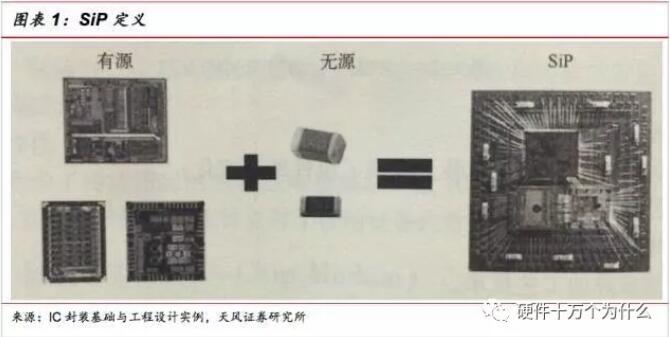
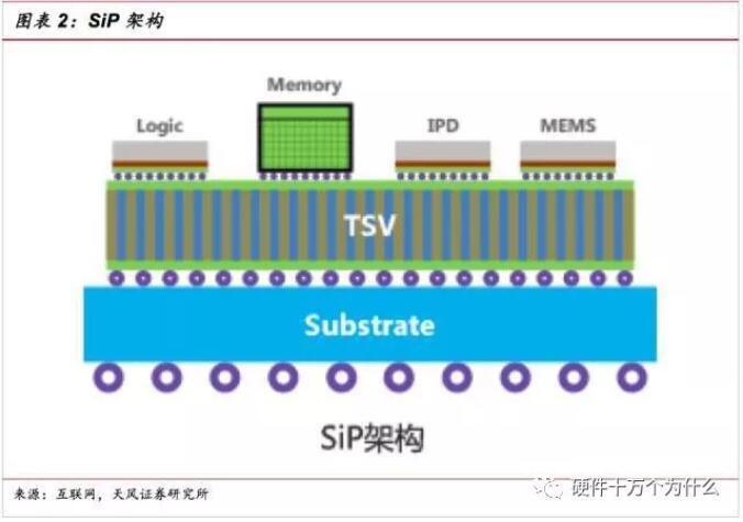
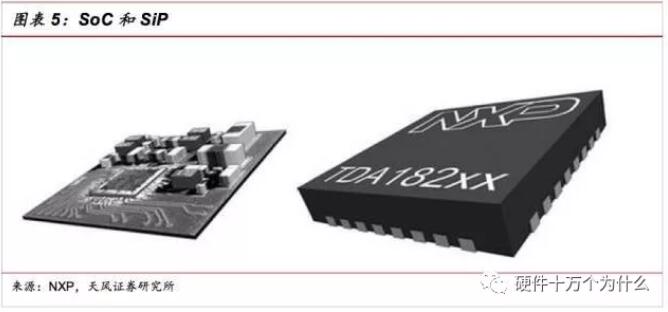
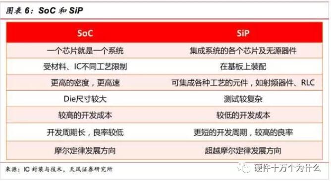
In terms of architecture, SiP integrates a variety of functional chips, including processors, memory and other functional chips in one package, so as to achieve a basically complete function. Corresponds to SOC (system on chip). The difference is that system-in-package is a packaging method in which different chips are used side by side or stacked, while SOC is a highly integrated chip product.
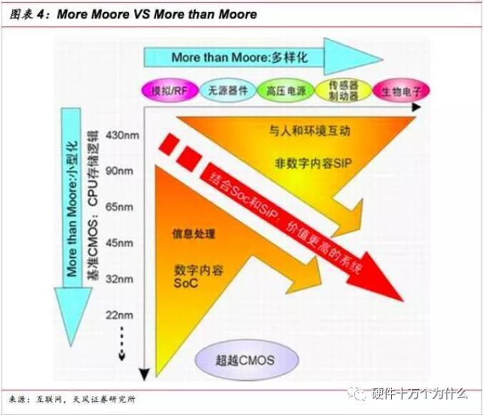
1.1. More Moore VS More than Moore——Comparison of SoC and SiP
SiP is an important realization path beyond Moore's Law. The well-known Moore's Law has developed to the present stage, where does it go? There are two paths in the industry: one is to continue to develop in accordance with Moore's Law. Products that follow this path include CPU, memory, logic devices, etc. These products account for 50% of the entire market. The other is the More than Moore route that surpasses Moore's Law. The development of chips has shifted from the blind pursuit of power consumption reduction and performance improvement to a more pragmatic approach to meeting the needs of the market. Products in this area include analog/RF devices, passive devices, power management devices, etc., accounting for about the remaining 50% of the market.
For these two paths, two products were born: SoC and SiP. SoC is the product of Moore's Law continuing to go down, and SiP is an important path to achieve beyond Moore's Law. Both are products that enable miniaturization and miniaturization of systems at the chip level.
SoC and SIP are very similar in that both integrate a system that includes logic components, memory components, and even passive components into a single unit. SoC is from a design point of view, which is to integrate the components required by the system into a single chip. SiP is a packaging method in which different chips are side-by-side or stacked from a packaging standpoint, and multiple active electronic components with different functions and optional passive devices, as well as other devices such as MEMS or optical devices are preferentially assembled together. , a single standard package that implements a certain function.
In terms of integration, in general, SoC only integrates logic systems such as AP, while SiP integrates AP+mobile DDR. To some extent, SIP=SoC+DDR. As the integration becomes higher and higher in the future, emmc is also likely to be integrated into SiP.
From the perspective of packaging development, SoC has been established as the key and development direction of future electronic product design due to the requirements of electronic products in terms of volume, processing speed or electrical characteristics. However, with the increasing cost of SoC production in recent years and frequent technical obstacles, the development of SoC is faced with a bottleneck, and the development of SiP has been paid more and more attention by the industry.
1.2. SiP - the inevitable choice path beyond Moore's Law
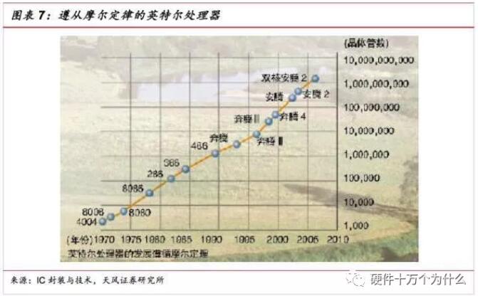
Moore's Law ensures continuous improvement in chip performance. As we all know, Moore's Law is the "Bible" for the development of the semiconductor industry. On silicon-based semiconductors, the feature size of transistors is halved and performance is doubled every 18 months. At the same time of performance improvement, it brings cost reduction, which makes semiconductor manufacturers have enough motivation to realize the reduction of semiconductor feature size. Among them, processor chips and memory chips are the two types of chips that most follow Moore's Law. Taking Intel as an example, each generation of products perfectly follows Moore's Law. At the chip level, Moore's Law promotes the continuous advancement of performance.
The PCB board does not follow Moore's Law and is the bottleneck for the performance improvement of the entire system. Corresponding to the continuous shrinking of the chip size, the PCB board has not changed much over the years. For example, the standard minimum line width of PCB motherboards is 3 mil (about 75 um) ten years ago, and it is still 3 mil today, with little improvement. After all, PCBs do not obey Moore's Law. Due to the limitation of the PCB, the performance improvement of the entire system has encountered a bottleneck. For example, since the PCB trace width has not changed, the wiring density between the processor and the memory also remains the same. In other words, the number of wires between the processor and memory will not change significantly without changing the size of the processor and memory package. The memory bandwidth is equal to the memory interface bit width multiplied by the memory interface operating frequency. The memory output bit width is equal to the number of connections between the processor and the memory. In the past ten years, 64bit has not changed due to the limitation of PCB board technology. Therefore, if you want to increase the memory bandwidth, you can only increase the operating frequency of the memory interface. This limits the performance improvement of the entire system.
SIP is the winner and loser in solving the shackles of the system. Encapsulate multiple semiconductor chips and passive devices in the same chip to form a system-level chip, instead of using the PCB board as the carrier between the connection between the carrier chips, which can solve the system performance caused by the inherent deficiencies of the PCB itself. encounter bottlenecks. Take processors and memory chips as an example, because the density of internal wiring in the system-in-package can be much higher than that of PCB wiring, so as to solve the system bottleneck caused by the broadband of PCB lines. For example, because the memory chip and the processor chip can be connected together by means of through holes, they are no longer limited by the PCB line width, so that the data bandwidth can be improved in the interface bandwidth.
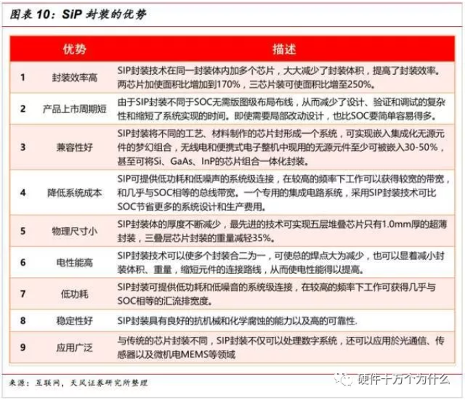
We believe that SiP is more than simply integrating chips together. SiP also has the advantages of short development cycle; more functions; lower power consumption, better performance, lower cost price, smaller size, and lighter weight. The summary is as follows:
SiP Process Analysis
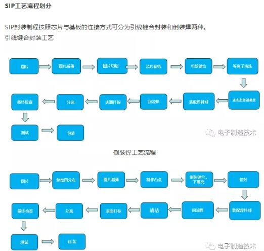
The SIP packaging process can be divided into wire bonding packaging and flip-chip bonding according to the connection method between the chip and the substrate.
2.1. Wire bonding packaging process
The main process of wire bonding packaging process is as follows:
Wafer → Wafer Thinning → Wafer Cutting → Die Bonding → Wire Bonding → Plasma Cleaning → Liquid Encapsulant Potting → Solder Ball Assembly → Reflow Soldering → Surface Marking → Separation → Final Inspection → Testing → Packaging.
wafer thinning
Wafer thinning refers to mechanical or chemical mechanical (CMP) grinding from the back of the wafer to thin the wafer to a level suitable for packaging. As the size of the wafer is getting larger and larger, in order to increase the mechanical strength of the wafer and prevent deformation and cracking during processing, its thickness has been increasing. However, with the development of the system in the direction of light, thin and short, the thickness of the module after chip packaging becomes thinner and thinner. Therefore, the thickness of the wafer must be reduced to an acceptable level before packaging to meet the requirements of chip assembly.
Wafer cutting
After the wafer is thinned, it can be diced. Older dicing machines were manually operated, and now general dicing machines are fully automated. Whether it is partially scribing or completely dividing the wafer, a saw blade is currently used because it draws neat edges with few chips and cracks.
die attach
The diced chips are mounted on the middle pads of the frame. The size of the pad should match the size of the chip. If the size of the pad is too large, the lead span will be too large, and the lead will be bent and the chip will be displaced due to the stress generated by the flow during the transfer molding process. The mounting method can be soldered to the substrate with soft solder (referring to Pb-Sn alloy, especially alloy containing Sn), Au-Si eutectic alloy, etc. The most commonly used method in plastic packaging is to use polymer adhesive. The adhesive is glued to the metal frame.
wire bonding
The lead used in the plastic package is mainly gold wire, and its diameter is generally 0.025mm~0.032mm. The length of the lead is usually between 1.5mm and 3mm, and the height of the arc can be 0.75mm higher than the plane where the chip is located.
Bonding techniques include thermocompression welding, thermosonic welding, etc. The advantages of these techniques are the ease of spherical formation (i.e. solder ball technology) and the prevention of gold wire oxidation. In order to reduce costs, other metal wires, such as aluminum, copper, silver, palladium, etc., are also being studied to replace gold wire bonding. The condition of hot pressure welding is that the two metal surfaces are in close contact, and the time, temperature and pressure are controlled to make the two metals connect. Rough surface (uneven), oxide layer formation or chemical contamination, moisture absorption, etc. will affect the bonding effect and reduce the bonding strength. The temperature of thermocompression welding is 300℃~400℃, and the time is generally 40ms (usually, plus the procedures such as finding the bonding position, the bonding speed is two wires per second). The advantage of ultrasonic welding is that it can avoid high temperature, because it uses 20kHz~60kHz ultrasonic vibration to provide the energy required for welding, so the welding temperature can be lowered. The simultaneous use of heat and ultrasonic energy for bonding is known as thermosonic welding. Compared with thermocompression welding, the biggest advantage of thermosonic welding is to reduce the bonding temperature from 350°C to about 250°C (some people think that the conditions of 100°C~150°C can be used), which can greatly reduce the bonding temperature on the aluminum pad. Possibility to form Au-Al intermetallic compounds, extending device lifetime while reducing circuit parameter drift. The improvement in wire bonding is mainly due to the need for thinner and thinner packages, some ultra-thin packages are onlyThere is about 0.4mm. Therefore, the lead loop (loop) is reduced from the general 200 μm~300 μm to 100 μm~125 μm, so that the lead tension is very large and very tight. In addition, there are usually two annular power/ground wires on the periphery of the wire pads on the substrate. To prevent the gold wire from short-circuiting with it during bonding, the minimum gap must be > 625 μm, and the bonding wire must have high linearity. degrees and a good arc.
Plasma cleaning
One of the important functions of cleaning is to improve the adhesion of the film, such as depositing an Au film on a Si substrate, and treating the surface of hydrocarbons and other contaminants by Ar plasma, which significantly improves the adhesion of Au. The surface of the substrate after plasma treatment will leave a layer of gray substance containing fluoride, which can be removed by solution. Simultaneous cleaning also helps to improve surface adhesion and wetting.
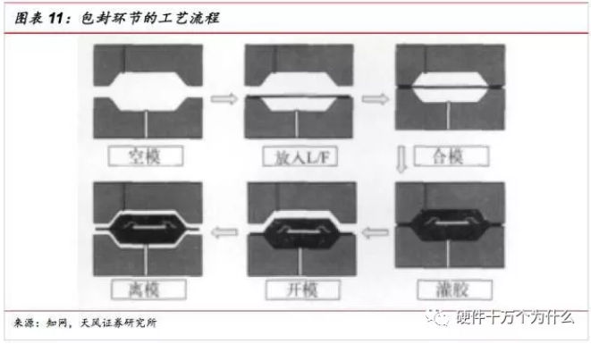
Liquid sealant potting
Place the chip mounted and wire-bonded frame tape in the mold, heat the pre-formed block of the molding compound in a preheating furnace (the preheating temperature is between 90°C and 95°C), and then put it into the transfer in the transfer tank of the molding machine. Under the pressure of the transfer molding piston, the molding compound is extruded into the runner and injected into the mold cavity through the gate (the mold temperature is maintained at about 170°C to 175°C throughout the process). The molding compound is rapidly solidified in the mold, and after a period of pressure holding, the module reaches a certain hardness, and then the module is ejected with the ejector pin, and the molding process is completed. For most molding compounds, after a few minutes of holding pressure in the mold, the module is stiff enough to allow ejection, but the curing (polymerization) of the polymer is not fully complete. Since the degree of polymerization (degree of curing) of the material strongly affects the glass transition temperature and thermal stress of the material, it is very important to promote the material to be fully cured to achieve a stable state, which is very important to improve the reliability of the device, and post-curing is to improve the molding compound The necessary process steps for the degree of polymerization, the general post-curing conditions are 170 ℃ ~ 175 ℃, 2h ~ 4h.
Liquid sealant potting
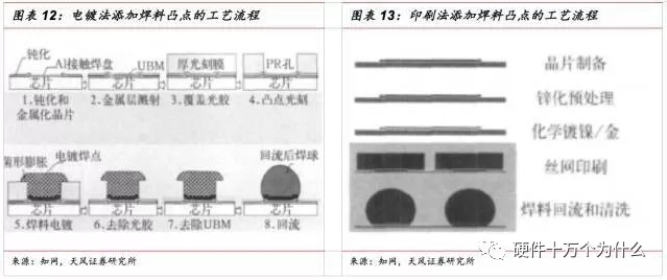
At present, there are two ball mounting methods used in the industry: "solder paste" + "solder ball" and "flux paste" + "solder ball". The "solder paste" + "tin ball" mounting method is recognized as the best standard ball mounting method in the industry. The balls planted by this method have good weldability and gloss, and the solder ball offset phenomenon will not occur during the tin melting process. It is easier to control. The specific method is to first print the solder paste on the BGA pad, and then use a ball-mounting machine or screen printing to add a certain size of solder balls. At this time, the role of the solder paste is to stick to the tin. When heating, the contact surface of the solder balls is larger, so that the solder balls are heated faster and more comprehensively, so that the solder balls have better solderability with the pads after melting and reduce the possibility of virtual soldering.
surface marking
Marking is the indelible and clear letters and logos printed on the top surface of the packaged module, including manufacturer's information, country, device code, etc., mainly for identification and traceability. There are many ways of coding, among which the most commonly used is the coding method, which includes ink printing and laser printing.
separate
In order to improve production efficiency and save materials, most SIP assembly work is carried out in the form of array combination, which is divided into individual devices after completing the molding and testing process. Dividing can be done by sawing or stamping. The sawing process is more flexible and does not require many special tools. The stamping process has higher production efficiency and lower cost, but requires the use of special tools.
2.2. Flip-chip welding process
Compared with the wire bonding process, the flip chip process has the following advantages:
(1) Flip-chip welding technology overcomes the problem of the center distance limit of wire bonding pads;
(2) It provides more convenience for electronic designers in the power/ground distribution design of the chip;
(3) By shortening the interconnection length and reducing the RC delay, it provides a more complete signal for high-frequency and high-power devices;
(4) Excellent thermal performance, a radiator can be installed on the back of the chip;
(5) High reliability, due to the action of the filler under the chip, the fatigue life of the package is enhanced;
(6) Easy to repair.
The following is the process flow of flip chip bonding (the same process as wire bonding will not be described separately): wafer → pad redistribution → wafer thinning, bump making → wafer cutting → flip chip bonding, Underfill→Encapsulation→Assembly Solder Balls→Reflow Soldering→Surface Marking→Separation→Final Inspection→Testing→Packaging.
Pad Redistribution
In order to increase the lead pitch and meet the requirements of the flip-chip bonding process, it is necessary to redistribute the leads of the chip.
make bumps
After the pad redistribution is completed, bumps need to be added to the pads on the chip. The solder bump fabrication techniques can be electroplating, electroless plating, evaporation, ball placement and solder paste printing. At present, the electroplating method is still the most widely used, followed by the solder paste printing method.
Flip-chip bonding, underfill
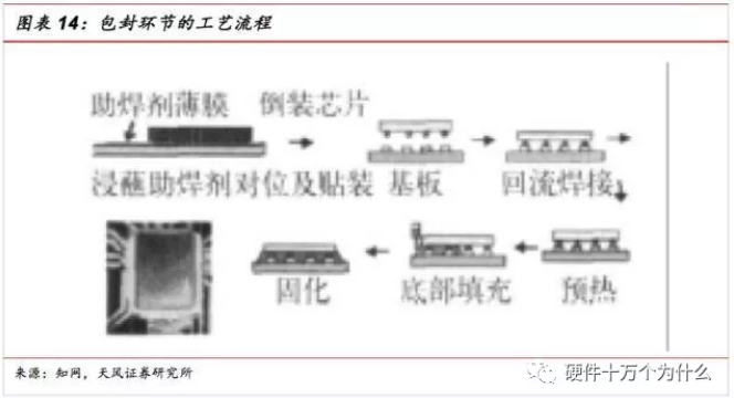
After the solder bumps are arranged on the entire chip bonding surface in the shape of the grid array, the chip is mounted on the package substrate in an inverted manner, and the electrical connection is achieved through the bumps and the pads on the substrate, replacing the WB and TAB. connection method. After flip-chip bonding, filling with epoxy resin between the chip and the substrate can reduce the thermal stress and mechanical stress applied to the bumps, and improve the reliability by 1 to 2 orders of magnitude compared with no filling.
SiP - for applications
3.1. Main application areas
The application of SiP is very extensive, mainly including: wireless communication, automotive electronics, medical electronics, computers, etc.
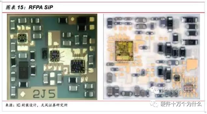
The most widely used wireless communication field. The application of SiP in the field of wireless communication is the earliest, and it is also the most widely used field. In the field of wireless communication, the requirements for functional transmission efficiency, noise, volume, weight and cost are getting higher and higher, forcing wireless communication to develop in the direction of low cost, portable, multi-function and high performance. SiP is an ideal solution that combines the advantages of existing core resources and semiconductor production processes, reduces costs, and shortens time-to-market, while overcoming difficulties in SOC such as process compatibility, signal mixing, noise interference, and electromagnetic interference. The radio frequency power amplifier in the mobile phone integrates the functions of the radio frequency power amplifier, power control and transceiver switch, which are completely solved in the SiP.
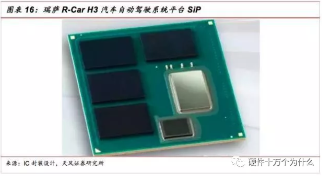
Automotive electronics is an important application scenario for SiP. SiP applications in automotive electronics are gradually increasing. Taking the engine control unit (ECU) as an example, the ECU consists of a microprocessor (CPU), memory (ROM, RAM), input/output interface (I/O), analog-to-digital converter (A/D), as well as large Scale integrated circuit composition. Different types of chips have different processes. At present, SiP is often used to integrate the chips into a complete control system. In addition, automobile anti-lock braking system (ABS), fuel injection control system, airbag electronic system, steering wheel control system, tire low pressure alarm system and other units, the use of SiP is also increasing. In addition, SIP technology has also been successfully applied in the fast-growing in-vehicle office systems and entertainment systems.
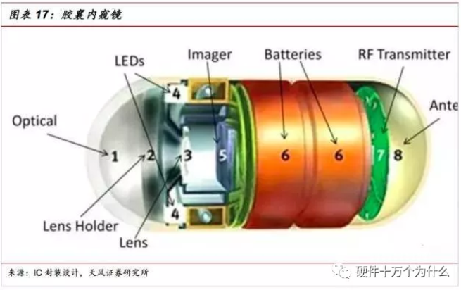
Medical electronics require a combination of reliability and small size, combined with functionality and longevity. Typical applications in this field are implantable electronic medical devices, such as capsule endoscopes. The endoscope is composed of an optical lens, an image processing chip, a radio frequency signal transmitter, an antenna, and a battery. The image processing chip is a digital chip, the radio frequency signal transmitter is an analog chip, and the antenna is a passive device. Packing these devices together in a SiP perfectly addresses performance and miniaturization requirements.
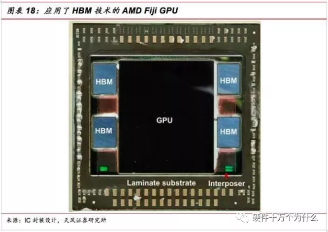
The application of SiP in the computer field mainly comes from integrating the processor and memory together. Taking GPU as an example, it usually includes graphics computing chip and SDRAM. The two packaging methods are not the same. Graphics computing is packaged in a standard plastic ball array multi-chip package, which is not suitable for SDRAM. Therefore, it is necessary to package the two types of chips separately, and then package them together in the form of SiP.
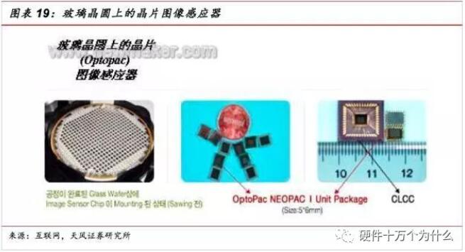
SiP also has many applications in other consumer electronics. This includes ISP (image processing chip), Bluetooth chip and so on. ISP is the core device of digital cameras, scanners, cameras, toys and other electronic products. It converts optical signals into digital signals through photoelectric conversion, and then realizes image processing, display and storage. Image sensors include a series of different types of components, such as CCD, CMOS image sensors, contact image sensors, charge loading devices, optical diode arrays, amorphous silicon sensors, etc. SiP technology is undoubtedly an ideal packaging technology solution.
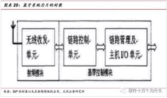
The Bluetooth system is generally composed of a wireless part, a link control part, a link management support part and a main terminal interface. SiP technology can make Bluetooth smaller and smaller to meet the needs of the market, thus vigorously promoting the application of Bluetooth technology. The SiP completes all the components (radio, baseband processor, ROM, filters, and other discrete components) required to integrate Bluetooth wireless technology functionality in an ultra-small package.
Electronic products have the characteristics of high performance, miniaturization, multiple varieties and small batches. SiP technology conforms to the application requirements of electronics, so it has a wide application market and development prospects in this technical field.
3.2.SiP - Tailored for Smartphones
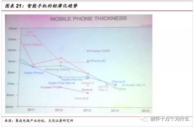
The thinning and lightness of mobile phones has brought about an increase in the demand for SiP. Mobile phones are the largest market for SiP packagingfield. As smartphones become thinner and lighter, the demand for SiP will naturally rise. From 2011 to 2015, the thickness of mobile phones of various brands has been continuously reduced. Thinning naturally has higher and higher requirements on the thickness of assembled components. Taking the iPhone 6s as an example, the use of PCB has been greatly reduced, and many chip components will be implemented in SiP modules. When it comes to the iPhone 8, it may be Apple's first mobile phone to use SiP. This means that on the one hand, the iPhone 8 can be made thinner and lighter, and on the other hand, there will be more space for other functional modules, such as more powerful cameras, speakers, and batteries.
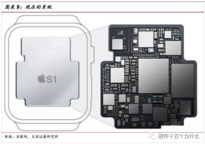
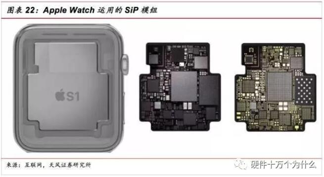
Look at SiP applications from Apple products. Apple is a company that is firmly optimistic about SiP applications. Apple has used SiP packaging on Apple Watch before.
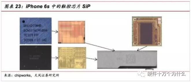
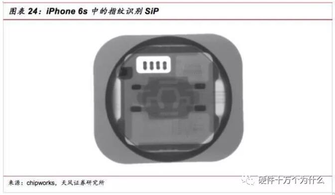
In addition to watches, the number of SiPs used in Apple mobile phones is also gradually increasing. Listed are: touch chip, fingerprint identification chip, RFPA and so on.
touch chip. In the Iphone6, there are two touch chips, which are provided by Broadcom and TI respectively, while in the 6S, the two are sealed in the same package to realize the SiP package. In the future, the entire TDDI will be further encapsulated. A new generation of 3D Touch technology was shown in the iPhone 6s. The touch sensing detection can penetrate the insulating material shell, and judge the touch action of the human finger by detecting the voltage change brought by the human finger, so as to realize different functions. The touch chip is to collect the voltage value of the contact point, convert these electrode voltage signals into coordinate signals after processing, and control the mobile phone to respond to the corresponding functions according to the coordinate signals, so as to realize its control function. The emergence of 3D Touch has put forward higher requirements for the processing capability and performance of the touch module. Its complex structure requires the touch chip to be assembled with SiP, and the tactile feedback function enhances its operational friendliness.
The fingerprint recognition also uses a SiP package. The sensor and control chip are packaged together, and similar technology has been adopted since the iPhone 5.
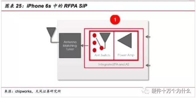
RFPA module. RFPA in cell phones is the most commonly used form of SiP. The iPhone 6S is no exception. In the iPhone 6S, there are multiple RFPA chips, all of which use SiP.
According to Apple's habit, all mature technologies will be passed on to the next generation. We judge that the upcoming Apple iPhone 7 will adopt SiP technology more, while the future iPhone 7s and iPhone 8 will be more comprehensive and use SiP technology to a greater extent. to compress the internal space.
The SIP packaging technology adopts a variety of bare chips or modules to be arranged and assembled. If the arrangement is distinguished, it can be roughly divided into a flat 2D packaging and a 3D packaging structure. Compared with 2D packaging, the use of stacked 3D packaging technology can increase the number of wafers or modules used, thereby increasing the number of layers in which wafers can be placed in the vertical direction, and further enhancing the functional integration capability of SIP technology. The internal bonding technology can be simple wire bonding (Wire Bonding), or flip chip bonding (Flip Chip), or a combination of the two.
From the current industry SIP design type and structure distinction, SIP can be divided into three categories.
2D SIP
This type of packaging is to package the chips one by one in a two-dimensional mode in a package body on the same packaging substrate.
Stacked SIPs
This type of packaging is a package that physically integrates two or more chip stacks in one package.
3D SIP
This type of packaging is based on 2D packaging, and multiple chips, packaged chips, multi-chips and even wafers are stacked and interconnected to form a three-dimensional package. This structure is also called stacked 3D packaging.
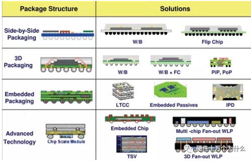
In addition, in addition to the 2D and 3D packaging structures, the method of integrating components on a multifunctional substrate can also be adopted - different components are embedded in the multifunctional substrate to achieve the purpose of functional integration. Different chip arrangements, combined with different internal bonding technologies, make the SIP package form a variety of combinations, and can be customized or flexibly produced according to the needs of customers or products.
The mainstream packaging form of SIP is BGA, but this does not mean that you have mastered SIP technology with traditional advanced packaging technology.
For circuit design, the three-dimensional chip package will have multiple die stacks, such a complex package design will bring many problems: such as the integration of multiple chips in one package, how to stack the chips; Layer substrate, it is difficult to route traces with traditional tools; there are also issues such as spacing between traces, equal-length design, and differential pair design.
In addition, with the increase of module complexity and the increase of operating frequency (clock frequency or carrier frequency), the difficulty of system design will continue to increase. In addition to the necessary design experience, the numerical simulation of system performance is also essential. design link.


Site Map | 萨科微 | 金航标 | Slkor | Kinghelm
RU | FR | DE | IT | ES | PT | JA | KO | AR | TR | TH | MS | VI | MG | FA | ZH-TW | HR | BG | SD| GD | SN | SM | PS | LB | KY | KU | HAW | CO | AM | UZ | TG | SU | ST | ML | KK | NY | ZU | YO | TE | TA | SO| PA| NE | MN | MI | LA | LO | KM | KN
| JW | IG | HMN | HA | EO | CEB | BS | BN | UR | HT | KA | EU | AZ | HY | YI |MK | IS | BE | CY | GA | SW | SV | AF | FA | TR | TH | MT | HU | GL | ET | NL | DA | CS | FI | EL | HI | NO | PL | RO | CA | TL | IW | LV | ID | LT | SR | SQ | SL | UK
Copyright ©2015-2025 Shenzhen Slkor Micro Semicon Co., Ltd
