Service hotline
+86 0755-83044319

release time:2023-12-25Author source:SlkorBrowse:21968
Zero Voltage Switching (ZVS) / Zero Current Switching (ZCS) technology, also known as soft-switching technology, can improve the efficiency of low-power soft-switching power supplies up to 80% to 85%. In the 1970s, resonant switching power supplies laid the foundation for soft-switching technology.
Basic Introduction
PWM switch-mode power supplies operate in a hard-switching mode, where the voltage and current waveforms overlap during the on/off process, resulting in large switching losses. Although high-frequency operation can reduce size and weight, switching losses are increased. Therefore, it is necessary to study technologies where the voltage/current waveforms do not overlap during switching, which is called ZVS/ZCS technology or soft-switching technology. The efficiency of low-power soft-switching power supplies can be improved to 80% to 85%. Resonant switching power supplies in the 1970s laid the foundation for soft-switching technology. Since then, new soft-switching technologies have emerged, such as quasi-resonant (in the mid-1980s), full-bridge phase-shifted ZVS-PWM, constant-frequency ZVS-PWM/ZCS-PWM (in the late 1980s), ZVS-PWM active clamp, ZVT-PWM/ZCT-PWM (in the early 1990s), full-bridge phase-shifted ZV-ZCS-PWM (in the mid-1990s), etc. China has already applied the latest soft-switching technology to 6kW communication power supplies with an efficiency of 98%.
Application of Technology
The key requirements for a buck regulator are usually size and efficiency. Because printed circuit board area is precious, no designer wants to allocate extra space to the power design solution. In addition, as microcontrollers and digital signal processors (DSPs) continue to evolve, circuit board design solutions also continue to upgrade. Although power has increased, product size cannot increase. Therefore, high-density regulators have been developed with the improvement of the latest IC integration, MOSFET technology, and packaging processes. Even so, these regulators still cannot meet the application requirements of new systems, especially as the power density within the system continues to increase. The main reason is that switching losses hinder the internal performance of the regulator's MOSFET. If these loss problems are not fundamentally solved, only minor performance improvements can be expected.
Reasons for Selection
The main causes of switching losses are: first, hard switching. Currently, most non-isolated buck regulator topologies have high switching losses. The reason is that during the on/off period, the MOSFET simultaneously bears high current and high voltage stress. When the switching frequency and input voltage increase, these losses also increase, limiting the maximum operating frequency, efficiency, and power density that can be achieved. Second, gate drive losses. Because the Miller charge in the gate drive circuit has a high power consumption, the gate drive losses of the hard-switching topology are also high. Third, body diode conduction. When the high-side MOSFET is turned on and off, high pulsating current flows through the body diode of the low-side MOSFET. The longer the conduction time of the body diode, the higher the reverse recovery loss and body diode conduction loss. Body diode conduction can also cause destructive overshoot and ringing. Switching losses also limit the switching frequency of the regulator. The higher the switching frequency, the longer the MOSFET switching time, and the greater the losses. If the switch cannot switch at a high frequency, the use of smaller passive components (resistors, capacitors, and inductors) will be limited, affecting the regulator density. Many electronic designers hope to use ZVS at the load point.
In response to these problems, Picor has introduced a high-performance, highly integrated, soft-switching buck regulator platform that can operate at high frequencies, greatly reducing switching losses and improving efficiency.
I. Background of ZVS Application
Zero Voltage Switching (ZVS) refers to when the switch tube is turned off, the voltage at both ends of the switch tube is already 0. This way, the switching loss of the switch tube can be minimized. The resonant power supplies we usually use, such as induction cookers and LLC power supplies, are all resonant power supplies. Ordinary chargers are hard-switched power supplies, which have higher losses than these resonant power supplies. Therefore, ZVS can achieve very high efficiency. For example, in an induction cooker, when we adjust the power to a relatively high level, it will continue to heat; when the power is adjusted to a lower level, it begins to intermittently heat because it cannot reach the resonant state. Hard-switching power supplies like our ordinary chargers always oscillate continuously regardless of whether they are loaded or unloaded. However, ZVS has one disadvantage, which is that its adjustment range is generally narrow.
II. Principles of Zero Voltage Switching (ZVS)
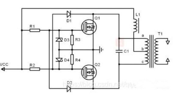
Figure 2-1 Zero Voltage Switching Principle Diagram (DC Power Supply)
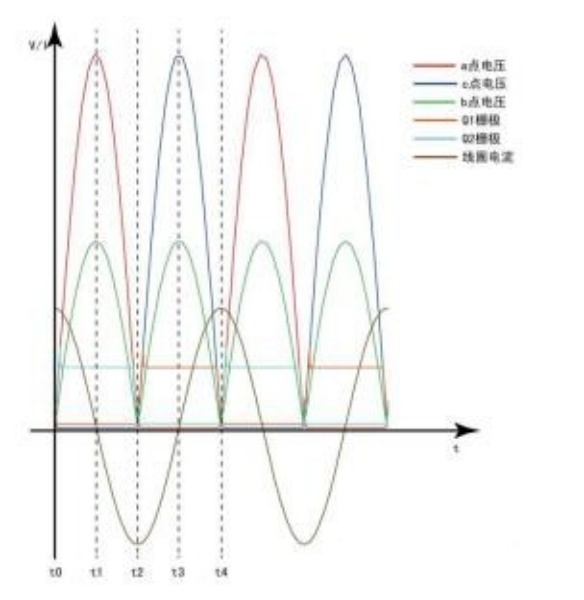
Figure 2-2 Zero Voltage Switching Waveform and Its Waveform at t2
When power is applied, the current flowing through L1 is zero. The power supply turns on Q1 and Q2 through R1 and R2, and the current through L1 gradually increases. Due to the differences in characteristics between the two switching transistors, the current flowing into Q1 and Q2 will be different. Assuming that the current through Q1 is greater than Q2, the gate voltage of Q1 will be higher than that of Q2. Through the diodes D1 and D2, the voltage at point 'a' will be lower than that at point 'c', resulting in an induced voltage with 'b' positive and 'a' negative. This forms positive feedback through T1, causing Q1 to turn on and Q2 to turn off, completing the start-up process.
(Time interval t0~t1) During steady state when Q1 is conducting, the previous period's current through T1 was from 'a' to 'c', and the voltage across C1 was zero. As current cannot change abruptly, the current through T1 charges C1, gradually resulting in a voltage across C1 with 'a' negative and 'c' positive, forming a growing sinusoidal waveform. At this time, voltage 'a' is pulled down to 0V by Q1, causing the voltage at point 'c' to increase sinusoidally. The gate voltage of Q1 is clamped by the voltage reference diode D3, keeping Q1 conducting in a clocked manner.
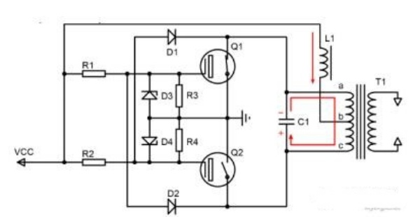
Figure 2-3 (t0~t1) Q1 Conducting, T1 Charging C1
3. (Time interval t1~t2) C1 starts to discharge through T1 from point 'c' to point 'a', causing the voltage across C1, i.e., the voltage at point 'c', to decrease sinusoidally. At the same time, the current through T1 increases sinusoidally from point 'c' to point 'a'.
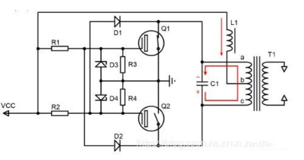
Figure 2-4 (t1~t2) Discharge of C1 to T1 winding, when the voltage across C1 is around 0, Q1 turns off and Q2 turns on.
4. (Time interval t2) When C1 is almost discharged, the voltage at point 'c' drops to around the threshold voltage of the MOS transistor, which causes Q1 to enter the amplification region through D2. At this time, the discharge current of C1 through the T1 winding from point 'c' to point 'a' reaches its maximum value. Simultaneously, as Q1 enters the amplification region, the voltage at point 'a' gradually rises, and Q2 also enters the amplification region through D1.
5. (Time interval t2) C1 is fully discharged, and the current through the T1 winding from point 'c' to point 'a' reaches its maximum value. It begins to charge C1, resulting in a voltage across C1 with 'a' positive and 'c' negative, while the voltage across C1 increases sinusoidally. At this time, both MOS transistors simultaneously enter the amplification region.
6. (Right figure) Due to continuous charging of C1 by T1, the voltage across C1 is positive at point 'a' and negative at point 'c'. Through the two diodes, the gate voltage of Q2 increases, and the gate voltage of Q1 gradually decreases, forming positive feedback. As a result, Q2 turns on and Q1 turns off.
7. The conduction process of Q2 is similar to that of Q1.
8. The inductance value of L1 is larger than that of T1, and the current through L1 remains relatively constant throughout the entire oscillation cycle. During the oscillation process, L1 continuously replenishes energy to the LC oscillator.
III. Zero Voltage Switching (ZVS) Calculation
1. Calculation of Waveform Amplitude
From the waveform graph, it can be seen that the waveform at point 'b' of L1 is the absolute value of a sine wave (i.e., the voltage that drops down to Vbm below). By using the steady-state condition where the voltage integral across the inductor is zero and the current integral across the capacitor is zero, the amplitude of the voltage at point 'b' can be calculated.
Assuming the voltage at point 'b' is  , and the voltage of the power supply is Vcc,
Then the voltage across both ends of L1 is therefore 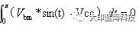 ,
,
Integrating the voltage across both ends of L1...calculated as ,
,
From the waveform graph, it can be observed that the voltage at point 'b' is half of the voltage between points 'a' and 'c'. Therefore, the voltage at the ends 'a' and 'c', which is also the voltage across C1, is...therefore, 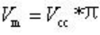 。
。
2. Calculation of Inductor Current
Once we know the voltage across the capacitor C1, is 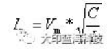 , we can calculate the maximum peak current in the inductor using the formulas for the energy stored in a capacitor and the energy stored in an inductor . The maximum peak current in the inductor is given by the formula: , where L is the inductance value between points 'a' and 'c'.
As we can see, with a larger value of capacitance (C) and a smaller value of inductance (L), the current through the inductor increases. This results in a stronger magnetic field and leads to electromagnetic induction heating. However, when the current through the inductor becomes too large, we need to consider the losses in its resistance. Additionally, the maximum current flowing through the capacitor is equal to the maximum current through the inductor. Therefore, when selecting the resonant capacitor, we need to take into account its maximum current rating.
3. Calculation of Resonant Frequency
Since this is an LC parallel resonance, the resonant frequency can be calculated as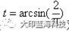
4. Calculation of AC Peak Current on Inductor L1
When the inductance value of L1 is relatively large, the current flowing through it is mainly DC, compensating for the energy lost in the oscillation. Since the amplitude at point 'b' is known, we can calculate the peak AC current in L1 during one oscillation cycle (the actual peak current is the sum of the DC current and the peak AC current).
The voltage at point 'b', Vb, equals Vcc for a duration of time, t:
Therefore, by integrating the voltage,, we can calculate the peak current flowing through L1. A small L1 will result in a large peak current, leading to unnecessary losses.
A 100W PD (Power Delivery) solution using the zero-voltage switching (ZVS) topology.
The increasing demand for larger battery capacity and shorter charging time has raised the requirements for charger power. Achieving high power in a small form factor poses a significant challenge, leading to various innovative solutions including the ZVS topology, high-performance switches, innovative packaging methods, and the use of wide-bandgap materials to meet the design requirements.
The objective is to achieve 94% efficiency and a power density of 23W/in3 by utilizing power switches and novel topology structures.
To achieve higher power density, it is necessary to select the appropriate topology structure, specifications, dimensions, and advanced control techniques. In the current high-power mobile charger market, there are multiple solutions available for high-power USB-PD chargers, including PFC+QR and PFC+LLC. However, these solutions have certain limitations, such as QR's inability to achieve soft-switching and the difficulty of using LLC topology for variable output voltage design.
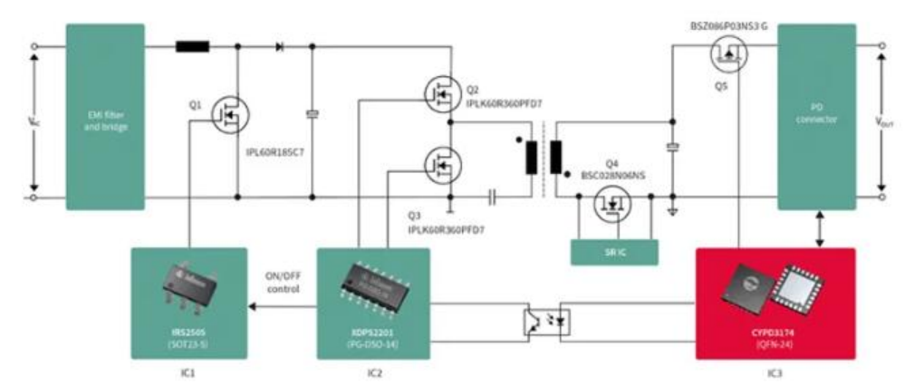
In response to these challenges, Infineon has introduced a new asymmetric half-bridge hybrid flyback topology (as shown in Figure 1). The half-bridge and series capacitor collectively drive the conventional flyback transformer. The main primary inductance of the flyback transformer and the series capacitor form a resonant circuit, which enables the ZVS characteristics of the half-bridge switches and provides resonant power transfer during the conventional demagnetization phase of the flyback transformer. During normal operation, the charging cycle and related power are controlled by peak DC current, while the demagnetization phase is controlled by timing to ensure proper negative pre-magnetization, thus meeting the required ZVS conditions for the half-bridge switches.
Figure 1: Simplified schematic diagram of the asymmetric half-bridge flyback topology.
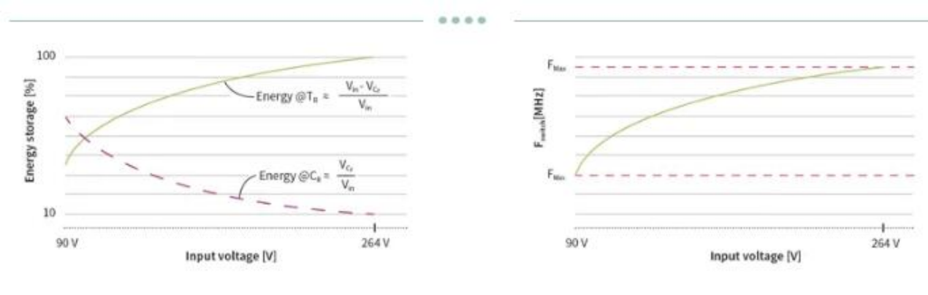
The power circuit on the primary side is implemented through an LC resonant circuit, which is driven by a half-bridge similar to an LLC converter. The resonant inductor Lr is a series inductor that can be either the leakage inductance of the transformer or the leakage inductance combined with an external inductor. Lm represents the main inductance of the transformer. The same conversion effect can also be achieved by connecting the resonant capacitor Cr and the primary coil of the transformer between the positive node and the midpoint of the half-bridge. When the high-side switch HS is conducting, energy will be stored in Cr and Lm, and the energy stored in each component will vary with the input voltage and switching frequency (as shown in Figure 2).
When the high-side switch HS is turned off, the current in the transformer will force the midpoint of the half-bridge VHB to drop until the body diode of the low-side switch clamps the voltage. Then, the low-side switch turns on at zero voltage while the transformer phase reverses, and energy is transferred to the secondary side. When the low-side switch turns off, the negative current induced in the transformer in the previous stage will force the voltage at the midpoint of the half-bridge VHB to rise until the body diode clamp voltage of the high-side switch HS, similar to the previous stage. Under ZVS conditions, HS is turned on while LS is turned off, but the current in the resonant circuit of the transformer is still negative, which means that the excess energy in the resonant circuit will be returned to the input end.
Why choose the hybrid flyback topology?
Compared with other flyback topologies, the hybrid flyback transformer needs to store less energy, which helps to reduce the size of the charger.
The hybrid flyback can achieve complete ZVS on the primary side and complete ZCS on the secondary side, and the leakage energy can also be recovered, thereby improving efficiency.
As shown in the following formula, the output voltage varies with the duty cycle. For the hybrid flyback, it is much easier to achieve a wide voltage range output, overcoming the limitations of the LLC topology in wide voltage output applications.
Vout: Output voltage
D: Duty cycle
Vin: Input voltage
Lm: Transformer inductance
N: Transformer turns ratio
Lr: Transformer leakage inductance
Infineon's 100W USB-PD reference design
The complete solution is shown in Figure 3. The PFC stage uses the critical conduction mode IRS2505 and ThinPAK package IPL60R185C7 CoolMOS™, while the DC-DC stage uses the digital PWM controller XDPS2201 and IPLK60R360PFD7. At the same time, the BSC028N06NS is used as a synchronous rectification switch (which can be replaced with the low-voltage ISZ0702NLS specifically designed for charger synchronous rectification in the future to further improve cost-effectiveness). The protocol controller is CYPD3174, and the p-channel MOS BSZ086N03NS3 is used as the output safety switch.
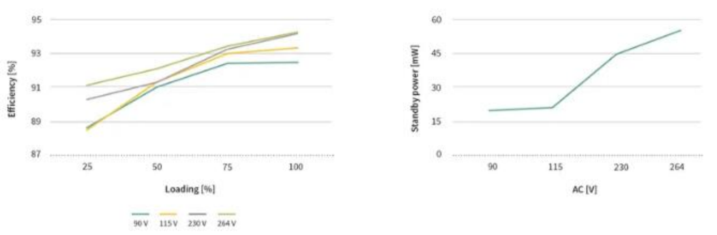
Through this configuration, the peak efficiency can reach 94%, and the standby power consumption is less than 60mW.
Highest Efficiency:
Choosing the right high-voltage MOSFET is crucial
Soft-switching technology allows the device to operate under Zero Voltage Switching (ZVS), where the MOSFET only turns on after its drain-source voltage reaches 0V (or close to 0V). This strategy eliminates conduction losses, which are typically the main contributors to total switch losses. Unfortunately, due to the "non-zero-loss" nature of the output capacitor, all high-voltage SJ MOSFETs suffer from an additional loss known as energy loss during the charging and discharging of the MOSFET output capacitance (Coss). Therefore, even when operating under ZVS conditions, it is not possible to recover all the energy stored in the output capacitor (Eoss). This phenomenon is related to the hysteresis characteristic of Coss, which can be observed through larger signal measurements during the Coss charging/discharging cycle. As a result, these losses are often referred to as Coss hysteresis losses (Eoss,hys).

Thanks to Infineon's advanced SJ technology, the CoolMOS™ PFD7 series further reduces hysteresis losses, thereby helping to improve efficiency even further.
Conclusion
Based on the digital XDPS2201, ZVS quasi-resonant topology can achieve ZVS and ZCS under different input voltage and output current conditions. Additionally, it can also recover energy from transformer leakage inductance. High-performance power MOSFETs contribute to achieving up to 94% efficiency in the 100W USB-PD design with dimensions of 60mm x 40mm x 18mm.


Site Map | 萨科微 | 金航标 | Slkor | Kinghelm
RU | FR | DE | IT | ES | PT | JA | KO | AR | TR | TH | MS | VI | MG | FA | ZH-TW | HR | BG | SD| GD | SN | SM | PS | LB | KY | KU | HAW | CO | AM | UZ | TG | SU | ST | ML | KK | NY | ZU | YO | TE | TA | SO| PA| NE | MN | MI | LA | LO | KM | KN
| JW | IG | HMN | HA | EO | CEB | BS | BN | UR | HT | KA | EU | AZ | HY | YI |MK | IS | BE | CY | GA | SW | SV | AF | FA | TR | TH | MT | HU | GL | ET | NL | DA | CS | FI | EL | HI | NO | PL | RO | CA | TL | IW | LV | ID | LT | SR | SQ | SL | UK
Copyright ©2015-2025 Shenzhen Slkor Micro Semicon Co., Ltd
