Service hotline
+86 0755-83044319

release time:2022-03-17Author source:SlkorBrowse:12153
One, refer to different
1. Source: referred to as FET. T is only conducted by majority carriers, which is the opposite of bipolar, also known as unipolar transistors.
2. Drain: Use the driving ability of the external circuit to reduce the internal driving of the IC, or drive a load higher than the chip power supply voltage.
Second, the principle is different
1. Source: A P-type region (represented by P+) with a high impurity concentration is diffused on both sides of an N-type semiconductor material to form two asymmetric P+N junctions. The two P+ regions are connected in parallel, and one electrode is drawn out, called gate (g), and one electrode is drawn out at each end of the N-type semiconductor.
2. Drain: Connect the lead lines of the two P regions together as an electrode, which is called gate, and lead out an electrode at each end of the N-type silicon wafer.
Extended information:
The principle of source structure
A P-channel junction field effect transistor can be made by diffusing an N+ region with a high impurity concentration on both sides of a P-type semiconductor. The above figure shows the structure diagram of this kind of tube and its representative symbol in the circuit. The type of channel can be confirmed by the direction of the arrow on the gate in the symbol represented by the junction field effect transistor.
The principle of drain structure
General transistors are conducted by carriers of two polarities, that is, majority carriers and minority carriers of opposite polarity, so they are called bipolar transistors, while FETs are only conducted by majority carriers. , which is the opposite of bipolar, also known as unipolar transistors.
It is a voltage-controlled semiconductor device with the advantages of high input resistance (108-109Ω), low noise, low power consumption, large dynamic range, easy integration, no secondary breakdown phenomenon, and wide safe working area. A strong competitor to polar transistors and power transistors.
Reference source:
Baidu Encyclopedia - Source
Reference source:
Baidu Encyclopedia-Drain
May I ask the origin of the gate, source and drain of the mos tube
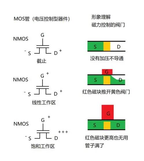
The gate is equivalent to a gate (switch) VG is greater than the VT tube conduction, the source is the place where the electrons come from, and the drain is the place where the electrons disappear (leak).
What is the difference between the source and drain of a MOS tube?
The polarity of the channel is the same as its drain and source, assuming the drain and source are ntype, then the channel will also be ntype
The dynamic MOS memory cell uses the gate capacitance of the MOS transistor to store information, so why is the charge preserved?
The dynamic MOS memory cell uses the gate capacitance of the MOS tube to store information, but because the capacity of the gate capacitance is very small, and the leakage current cannot be absolutely equal to 0, the charge storage time is limited.
What is the role of drain, source and gate of FET?
The source potential of the FET is higher than the gate potential (about 0.4V).
Field effect transistors use majority carriers for conduction, so they are called unipolar devices, while transistors have both majority carriers and minority carriers for conduction, and are called bipolar devices.
The source and drain of some FETs can be used interchangeably, and the gate voltage can also be positive or negative, which is more flexible than transistors.
The field effect transistor can work under the condition of very small current and very low voltage, and its manufacturing process can easily integrate many field effect transistors on a silicon wafer, so the field effect transistor has been widely used in large-scale integrated circuits. Wide range of applications. To-3p is an in-line package, the side with the word faces itself, and the pins are downward, so that from left to right are g, c, and e.
where g is the gate,
c is the collector, equivalent to d drain,
e is the emitter, which is equivalent to the s source.
What is the difference between source and drain of MOS?
1. Difference: source (source) source resource, power supply, Chinese translation is source. An electrode that acts as a collector. Drain (drain) drain drain, leak, Chinese translation is drain. Electrodes that act as emitters.
2. The mos tube is a metal-oxide-semiconductor field effect transistor, or a metal-insulator-semiconductor. The source and drain of the MOS tube can be reversed, and they are all N-type regions formed in the P-type backgate. In most cases, these two regions are the same, even if the two ends are reversed, it will not affect the performance of the device. Such devices are considered symmetrical. Definition of mos tube: The structure of the field effect tube is to use impurities to diffuse out a high concentration p-type region on both sides of an n-type semiconductor, which is represented by p+ to form two p+n junctions. Two electrodes are drawn from both ends of the n-type semiconductor, which are called drain d and source s, respectively. The p-regions on both sides are drawn out of the electrodes and connected together as gate g. If a forward voltage is applied between the drain and the source, the many subs (that is, electrons) in the n region can conduct electricity. They start from the source s and flow to the drain d. The direction of the current from d to s is called the drain current id. Since the conductive channel is n-type, it is called an n-channel junction field effect transistor.
The drain and source electrodes of field effect transistors (including junction type and insulated gate type) are usually made symmetrical, and the drain and source electrodes can be used interchangeably.
But some insulated gate field effect transistors are making products
The source and substrate are connected together
, so the source and drain of this tube cannot be interchanged. Some tubes lead the substrate to a single pin to form four pins. In general, the p substrate is connected to a low potential, and the n substrate is connected to a high potential. MS has no essential difference at the level of semiconductor materials. At that time, in the design of semiconductor devices, the substrate electrode was generally connected to the source electrode, so the switching performance of MOSFET was related to V_{GS}, as long as V_{GS} exceeded the threshold value, it would lead to On/off (depending on depletion mode or enhancement mode) So essentially S, D are determined by the way the semiconductor device is internally connected. So reverse connection will cause a short circuit


Site Map | 萨科微 | 金航标 | Slkor | Kinghelm
RU | FR | DE | IT | ES | PT | JA | KO | AR | TR | TH | MS | VI | MG | FA | ZH-TW | HR | BG | SD| GD | SN | SM | PS | LB | KY | KU | HAW | CO | AM | UZ | TG | SU | ST | ML | KK | NY | ZU | YO | TE | TA | SO| PA| NE | MN | MI | LA | LO | KM | KN
| JW | IG | HMN | HA | EO | CEB | BS | BN | UR | HT | KA | EU | AZ | HY | YI |MK | IS | BE | CY | GA | SW | SV | AF | FA | TR | TH | MT | HU | GL | ET | NL | DA | CS | FI | EL | HI | NO | PL | RO | CA | TL | IW | LV | ID | LT | SR | SQ | SL | UK
Copyright ©2015-2025 Shenzhen Slkor Micro Semicon Co., Ltd
