Service hotline
+86 0755-83044319

release time:2022-03-17Author source:SlkorBrowse:12612
1: Moore's Law
In 1965, the legend of Silicon Valley, one of the "Eight Traitors" of Fairchild, the former CEO and honorary chairman of Intel, and the great discoverer of laws, Gordon · Moore, was preparing a report on the development trend of computer memory.
When he started plotting the data, he noticed a surprising trend.
Each new chip contains roughly twice the capacity of its predecessor, and each chip is produced within 18 to 24 months of the previous chip. If this trend continues, computing power relative to the time period will increase Exponential rise.
This is the famous Moore's Law, and its description of the development of the integrated circuit industry is unusually correct.
to conclude:
1: The number of circuits integrated on an integrated circuit chip (wafer) doubles every 18 months.
2. The performance of the microprocessor doubles every 18 months, while the price drops by half.
3. The computer performance that a dollar can buy quadruples every 18 months.
You might think that Moore's Law is nothing but a summary?
In fact, this can deduce a formula, that is, every 18 months, the chip area is halved when the chip size remains unchanged.
In this way, wafers of the same size can produce twice as many chips.
If the chip area of the previous generation process is 1mm2, in the new process, the area is half of the new process, which is 0.5mm2.
We assume that the cost of the two generations of wafers is the same (generally, the new process will be more expensive), then the cost of the new process is half of the original process cost.
This is the reality revealed by Moore's Law:
That is, the chip using the new process has a smaller area, better power consumption, higher frequency and lower cost.
This is the dimensionality reduction attack of the new technology on the old technology!
These advantages and benefits are the engine that drives the continuous advancement of chip technology.
That is the connotation of Moore's Law.
If the chip technology advances, the size of each transistor will shrink. How much does it shrink?
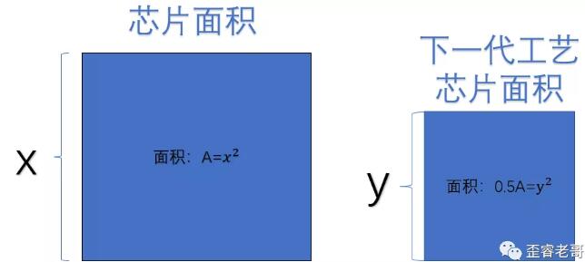
As shown in the figure above, while the number of transistors remains the same, the chip area of the next-generation new process is half of the previous generation.
So what is the relationship between X and Y?
What if we counted in terms of squares?
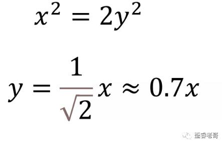
Then the new process is about 0.7 times the size of the transistors of the old process.
That is, the transistor will be 0.7 times smaller.
According to Moore's Law, we can use the mathematics knowledge of junior high school to calculate the progress of each generation of technology, starting from 800nm (this 80586 process node).
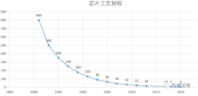
The development of chip technology also confirms this:
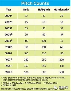
From 0.8 μm, 0.5 μm, 0.35 μm, 0.25 μm, 0.18 μm, 0.13 μm, 90 nm, 65 nm, 45 nm, 32 nm, 22 nm, 16 nm, 10 nm, 7 nm, 5 nm.
The actual process node meets this requirement.
Moore's Law is completely consistent with the current chip manufacturing process.
magic!
2: Half node
Some students with process knowledge may say:
Something is wrong,
In this picture, where did the hot 40nm, 28nm, and 14nm process go.
Yes, this involves a common method used by chip manufacturers.
shrink.
We all know that after a process node is successfully developed, its research and development costs are very high.
If you can continue to optimize on this process node, area, power consumption, etc.
It is also a way to maximize the use of existing investment.
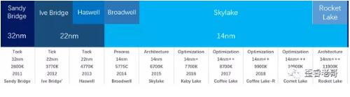
Just like what Intel did on 14nm.
14nm+++
Continuous optimization.
And the shrink we are talking about today is also an optimization.
It is essentially proportionally scaled with the use of lighting (MASK). The transistor size is reduced a little, and the chip can still work normally, thereby reducing the chip area and reducing the cost.
So what is the shrink ratio?
Shrink typically reduces the size of transistors by a factor of 0.9.
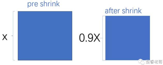
Approximately each side length is scaled by 0.9; the overall area is reduced by 0.81;
This process is also known as die shrink.
However, scaling down may introduce new problems, such as increased leakage current, but the leakage current can be adjusted by process parameters. Shrink can also tap the potential of this process node without changing the process characteristics.
These shrinked process nodes are also called half nodes.
E.g:
40nm is the half node after 45nm shrink.
28nm is the half node after 32nm shrink.
20nm is the half node after 22nm shrink.
14nm can also be regarded as a half node after 16nm shrink.
Multiply the previous process by 0.9.
DIE shrink is done by chip manufacturers and has nothing to do with chip design companies.
The layouts designed by engineers are all pre-shrinked, and when the manufacturer produces them, they are directly shrinked, and the area of the generated die is proportionally smaller than the version.
So our chip design engineers now have a shrinking process when doing half-node processes such as 40nm or 28nm.
It will be found that the layout of the chip is larger than the actual DIE area.
If we calculate the final DIE (chip) area, it is actually the area after shrink, not the area of the layout.
The EDA tool marks the area before shrink (pre shrink).
That is, the design company gave the chip factory a 10X10 design drawing, but the chip factory produced a 9x9 size.
For the specific definitions of DIE, WAFER, etc., for unfamiliar students, you can refer to "Those "speaking words" of high-quality human chip engineers originally written by my brother"
These optimized ones, 40nm, 28nm, etc., have become more mature and long-lived processes.
The original 45nm, 32nm, etc., compared with the optimized 40nm, 28nm, no longer have advantages, manufacturers no longer promote these processes.
In fact, the industry usually regards the 45nm/40nm, 32nm/28nm, 22nm/20nm, 16nm/14nm process nodes as the same process node, which is a generation, but is optimized by manufacturers through shrinking.
After adding shrink, we see the current 28nm, 14nm, 10nm, 7nBoth m and 5nm can be calculated using the mathematics knowledge of junior high school in the previous section of Moore's Law.
Strictly fit, theory and practice are in good agreement.
Gordon Moore, what a genius!
3: Gate length
But is this really the case?
There is a great hidden meaning in these figures.
Let's look at a picture:
From about the 1960s to the late 1990s, nodes were named based on their gate length. This diagram from IEEE shows the following relationship.
The gate length and half-pitch (half the distance between two identical features on the chip) match the process node name, which is why 0.5um, 0.35um, 0.25um are actually named.
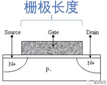
But below 28nm, due to the use of new technologies such as finfet, these do not match the actual node and gate length and half-pitch.
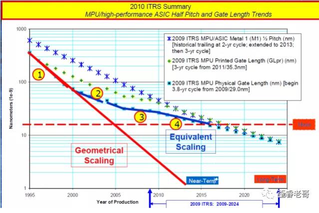
If you keep the node name and the actual feature size in sync, it will appear as the red line.
Before 2015, the minimum process size for chip manufacturing will fall below 1nm.
In fact, the manufacturer secretly crossed the warehouse,
In reality, the entire process curve is closer to that shown by the blue line.
The 7nm and 5nm you thought were no longer the gate length or half-pitch.
So how did 7nm and 5nm come about?
Draw a pie!
Draw a pie, are you familiar with this?
The boss of the company is best at doing this, drawing a pie, or drawing a roadmap.
The boss said: It will double every year in the next three years. This year, the sales will be 100 million. In 10 years, it will become a company with sales of 100 billion.
The point is, this thing can't be calculated like this. According to this calculation, after a few decades, the earth will become your company's, and your sales will not be completed.
So how is the chip manufacturing pie, or (roadmap) drawn?
Because semiconductor manufacturing involves huge capital expenditures and a lot of long-term research. The average time from introduction of a new technical method in a paper to large-scale commercial manufacturing is about 10-15 years.
Decades ago, the semiconductor industry recognized that if there was an overall roadmap for the introduction of nodes and the functional sizes that those nodes would address, that would guide every unit involved in the chip flow.
That is to say, for example, in 2025, we will draw a big pie to develop 1nm. Then, the lithography equipment manufacturers, etching equipment manufacturers, material manufacturers, research institutions, etc. that are needed at this time must aim at this goal.
This roadmap is primarily intended to "provide a major future reference for universities, consortia and industry researchers to stimulate innovation in various technological fields".
In other words, it is necessary to draw a big pie for chip manufacturing practitioners.
Over the years, the International Technology Roadmap for Semiconductors (ITRS) has published an overall roadmap for the industry. These roadmaps span 15 years and set overall goals for the semiconductor market.
ITRS is the one who draws the pie!
How to draw this roadmap?
Moore's Law, of course, as described in the first part of this article.
Moore's Law is so rude.
Has been from a few hundred nm, dry to 5nm or 3nm.
The point is, math can do this, but can physics do it?
It's a bit too hasty to do this.
4: Marketing Means: BMW 5 Series and 5nm
Soon after, the ITRS (International Technology Roadmap for Semiconductors) organization also understood that this is not acceptable.
The reasons why you cannot relate gate length or half-pitch to node size are:
So these dimensions either stop scaling or scale more slowly.
Brutally multiply by 0.7 and expect the transistor to work.
Such transistors cannot be manufactured by the industry.
So, in 2010, ITRS collectively referred to the technology on each node as "equivalent scaling".
In other words, you don't need to actually correspond, you think it's not bad.
That is to say, 7nm and 5nm are no longer the gate length or half-pitch that they originally referred to.
This change reflects the status quo of the chip manufacturing industry:
"It used to be a technology node, a node number, that meant something, some function on a wafer," [敏感词]'s Philip Wong said during the Hot Chips 31 keynote.
But: "Today, the numbers are just numbers. They're like car models - like a BMW 5 Series or a Mazda 6. It doesn't matter what the number is, it's just the destination of the next technology, its name. So we Don't confuse the name of the node with what the technology actually provides."
Drawing point: don't confuse the name of the node with the actual technology
5nm and 7nm are no different from BMW 5 and Mazda 6.
These are just marketing tactics.
It's not that the public is going to confuse the name.
It's these chip manufacturers, who use these marketing words to confuse the nodes of the process and the actual size of the transistors?
Although the big ship Moore's Law entered the shallow waters, it was about to run aground.
Let's rock this big ship together and move on as Moore's Law says,
So someone at Intel came up with it.
Don't talk about it, 5nm, 7nm, let's directly compare the number of transistors per unit area.
Here is the formula:
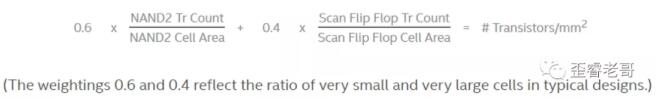
Intel's chip manufacturing expert, Mark Bohr, believes that every chip maker should disclose its logic transistor density in MTr/mm2 (millions of transistors per square millimeter) when referring to a process node.
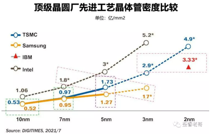
This also explains why Intel's 10nm and [敏感词]'s 7nm, although they seem to be two generations, have basically the same transistor density.
However, this formula is too complicated.
How is it possible that 7nm and 5nm have a good publicity effect on the public.
But, to be honest, Intel itself doesn't really follow the gate length (gate length) model in its own naming scheme.
From the table below, as the craft progresses, there are fewer and fewer players.
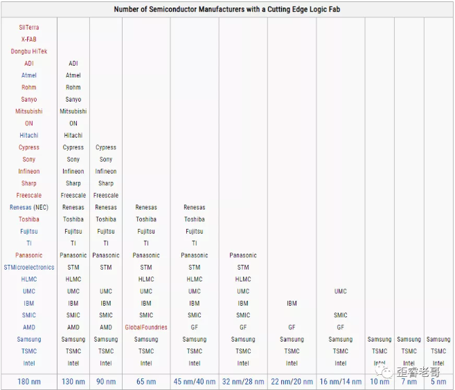
The high-end players are left with [敏感词] and Samsung, and Intel, which has been catching up.
Next year, Samsung and [敏感词]'s 3nm are both claiming to be mass-produced.
But this time, we should know that this is just a generation process code name, and has nothing to do with 3nm itself.
From 7nm, 5nm, to 3nm.
Moore's Law is not dead.
only,
Faltering, and getting old.
Citation:
1: Technology Node - WikiChip
2: How Are Process Nodes Defined? - ExtremeTech
3: [敏感词]’s 7nm, 5nm, and 3nm “are just numbers… it doesn’t matter what the number is” | PCGamesN
Disclaimer: This article is reproduced from "Luke Verification", this article only represents the author's personal views, not the views of Sac Micro and the industry, only for reprinting and sharing, support To protect intellectual property rights, please indicate the original source and author for reprinting. If there is any infringement, please contact us to delete it.


Site Map | 萨科微 | 金航标 | Slkor | Kinghelm
RU | FR | DE | IT | ES | PT | JA | KO | AR | TR | TH | MS | VI | MG | FA | ZH-TW | HR | BG | SD| GD | SN | SM | PS | LB | KY | KU | HAW | CO | AM | UZ | TG | SU | ST | ML | KK | NY | ZU | YO | TE | TA | SO| PA| NE | MN | MI | LA | LO | KM | KN
| JW | IG | HMN | HA | EO | CEB | BS | BN | UR | HT | KA | EU | AZ | HY | YI |MK | IS | BE | CY | GA | SW | SV | AF | FA | TR | TH | MT | HU | GL | ET | NL | DA | CS | FI | EL | HI | NO | PL | RO | CA | TL | IW | LV | ID | LT | SR | SQ | SL | UK
Copyright ©2015-2025 Shenzhen Slkor Micro Semicon Co., Ltd
