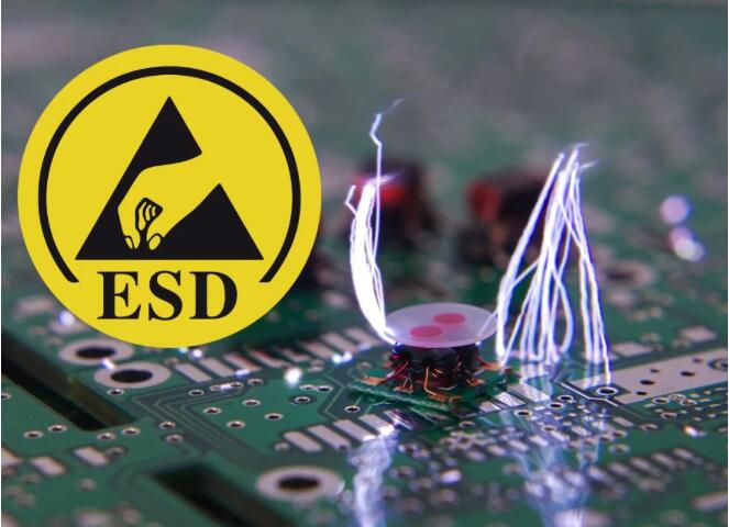
Let's talk about what ESD: Electrostatic Discharge (ESD)? This should be the main culprit of excessive electrical stress damage caused by all electronic components or integrated circuit systems. Because static electricity usually has a very high instantaneous voltage (> several thousand volts), this kind of damage is devastating and permanent, which will cause the circuit to burn directly. Therefore, the prevention of electrostatic damage is the number one problem in all IC design and manufacture.Static electricity is usually generated artificially, such as the process of production, assembly, testing, storage, handling, etc., which may cause static electricity to accumulate in the human body, instruments or equipment, and even the components themselves. When people contact these charged objects unwittingly, a discharge path will be formed, which instantly damages the electronic components or systems by electrostatic discharge (this is why before repairing computers, wrist strap must be worn on the working table. Chip to prevent electrostatic damage to human body), just as the charge stored in the clouds instantly breaks through the clouds to produce violent lightning, which will split the earth, and it is usually in rainy days, because the air humidity is so high that it is easy to form conductive leads.
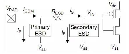
So, how to prevent electrostatic discharge damage? Of course, first of all, change the environment and reduce static electricity from the source (such as reducing friction, wearing less wool sweaters, controlling air temperature and humidity, etc.). Of course, this is not the focus of our discussion today.Today, we are going to discuss how to involve the protection circuit in the circuit. When there is static electricity outside, our electronic components or systems can protect themselves from being damaged by static electricity (in fact, installing a lightning rod). This is also the number one problem for many IC designers and manufacturers. Many companies have teams specializing in ESD design. Today, I will talk to you about the basic theory and explain the principles and points for attention of ESD protection step by step. You will find that the PN junction/diode, triode, MOS tube and snap-back mentioned earlier are all used. . .When the previous topic explained the theory of PN junction diode, it was said that the diode has a characteristic: forward conduction and reverse cut-off, and when the reverse bias voltage continues to increase, avalanche breakdown will occur and conduction will occur. We call it Clamp diode. This is the theoretical basis that we need to design electrostatic protection. We use this reverse cut-off feature to make this bypass open during normal operation, and when there is static electricity outside, this bypass diode will avalanche and form a bypass path to protect the internal circuit or grid (is it similar to that there is an overflow in the sink at home to prevent the whole bathroom from flooding when the faucet is left off).Then the question is, is this breakdown of this protection circuit completely dead? Is it a one-time thing? Of course not. The breakdown of PN junction is divided into two types, namely, electric breakdown and thermal breakdown. Electric breakdown refers to avalanche breakdown (low concentration) and zener breakdown (high concentration), and this electric breakdown is mainly due to the collision ionization of carriers to produce new electron-hole pairs, so it can be recovered. However, the thermal breakdown cannot be recovered, because the heat accumulation causes the silicon (Si) to be melted and burned. Therefore, we need to control the current at the moment of conduction. Generally, a high resistance is connected in series with the protection diode.In addition, can you understand by analogy why the ESD area can't form Silicide? There is also a theory for everyone. ESD is usually next to the Pad at the input of the chip, but not inside the chip, because we always hope that the external static electricity needs to be discharged at the first time. There will be a delay in putting it inside (pay attention to the chip that I dissected earlier. There are diodes next to the PAD. There are even two levels of ESD, so as to achieve the purpose of double protection.
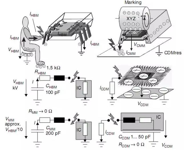
Before we talk about the principle and Process of ESD, let's talk about ESD standards and test methods. According to the generation mode of static electricity and the damage mode to the circuit, there are usually four test methods HBM: Human-Body Model (HBM), Machine Model (CDM), charge-device model (CDM) and field-induced model (FIM). However, the industry usually uses the first two modes to test (HBM, MM).
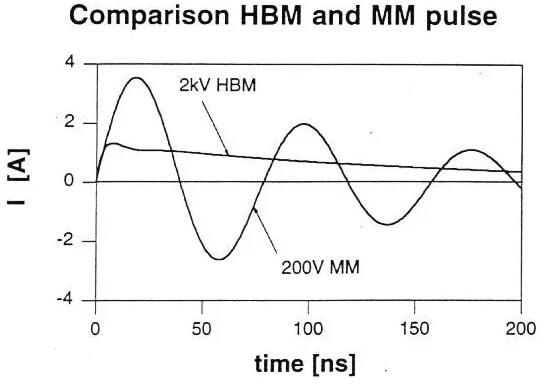
1. Human body discharge mode (HBM): Of course, the electric charge generated by human body friction suddenly hits the electric charge released by the chip, which causes the chip to burn down and breakdown. Touching with others in autumn often leads to electric shock. There are also traces of ESD standards for HBM in the industry (MIL-STD-883C method 3015.7, equivalent human capacitance is 100pF, equivalent human resistance is 1.5Kohm), or the international electronic industry standard (EIA/JESD22-A114-A), depending on which one you want to follow. If it is MIL-STD-883C method 3015.7, it stipulates that it is Class-1 if it is less than 2kV, class-2 if it is 2 kV to 4 kV, and class-3 if it is 4 kV to 16 kV. 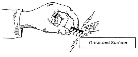 2. Machine discharge mode (MM): Of course, the static electricity generated by the machine (such as robot) is released by the pin when it touches the chip. The sub-standard is EIAJ-IC-121 method 20 (or standard EIA/JESD22-A115-A), and the equivalent machine resistance is 0 (because of metal), and the capacitance is still 100pF. Because the machine is metal and the resistance is 0, the discharge time is very short, almost between ms or us. But more importantly, because the equivalent resistance is 0, the current is very large, so even 200V MM discharge is more harmful than 2kV HBM discharge. Moreover, because there are many wires in the machine itself that will couple with each other, the current will interfere with the change with time.
The ESD test method is similar to the GOI test in FAB. After specifying the pin, give it an ESD voltage, and after a period of time, then come back to test the electrical property to see if it is damaged. No problem, add another step ESD voltage for a period of time, and then test the electrical property. This is repeated until the breakdown, and the breakdown voltage at this time is the ESD failure threshold Voltage. Usually, we apply voltage (3 zaps) to the circuit three times. In order to reduce the test cycle, the initial voltage is usually 70% ESD threshold of the standard voltage, and each step can be adjusted by itself by 50V or 100V as required.
|
(1). Stress number = 3 Zaps. (5 Zaps, the worst case)
|
|
(2). Stress step
|
ΔVESD = 50V(100V) for VZAP <=1000V
ΔVESD = 100V(250V, 500V) for VZAP > 1000V
|
|
(3). Starting VZAP = 70% of averaged ESD failure threshold (VESD)
|
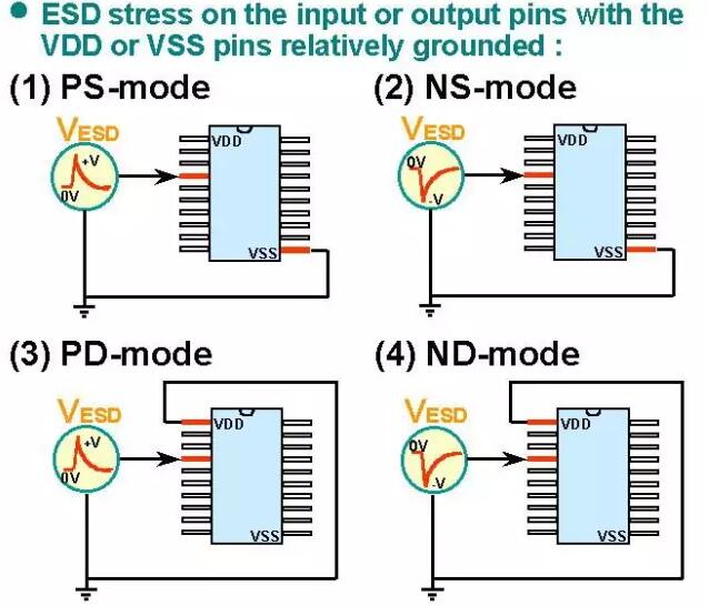
In addition, because there are many pin pins in each chip, whether you are one pin test or a combination pin test, it can be divided into several combinations: I/O-pin test (Input and Output pins), pin-to-pin test, Vdd-Vss test (input to output), and Analog-pin.1. I/O pins: ESD tests are conducted on input-pin and output-pin respectively, and there are four combinations: input+ positive charge, input+ negative charge, output+ positive charge and output+ negative charge. When testing input, the output and other pins are all floating, and vice versa.
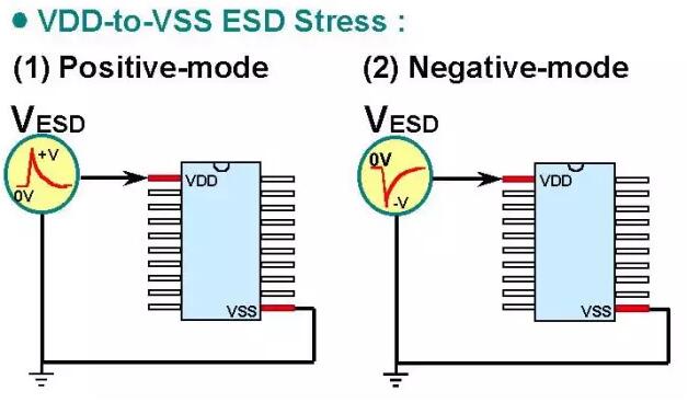
2. pin-to-pin test: electrostatic discharge occurs between pin-to-pin to form a loop, but if there are too many combinations of two pin tests, because any I/O must first go through VDD/Vss to supply power to the whole circuit if it is to affect the whole circuit, so the improved version uses a certain I/O-pin to add positive or negative ESD voltage, and all other I/Os are grounded together, but the input and the output are grounded. 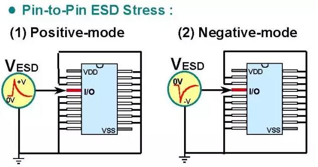 3. Electrostatic discharge between Vdd and Vss: It is only necessary to connect Vdd and Vss, and all I/O is floating, so that static electricity can pass between VDD and VSS.
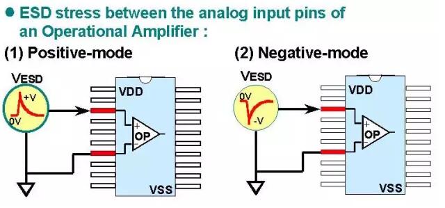
4. Analog-pin discharge test: Because many Differential Pair or operational amplifiers (OP AMP) in analog circuits have two inputs, it is necessary to do ESD test separately, that is, only for these two pins, and all other pins are floating.
Ok, that's it for the principle and test of ESD. Next, let's talk about Process and design factor.With the further reduction of Moore's law, the device size is getting smaller and smaller, the junction depth is getting shallower and the GOX is getting thinner, so it is easier to ride through the electrostatic shock. Moreover, in the Advance process, the introduction of Silicide will also make the electrostatic breakdown sharper, so almost all chip designs have to overcome the electrostatic breakdown problem.
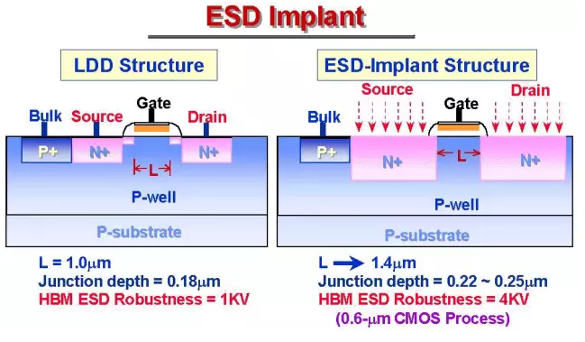
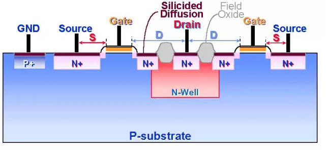
Electrostatic discharge protection can be solved from the Process on the FAB side or designed from the Layout on the IC design side, so you will see that Prcess has an ESD option layer, or the Design rule has ESD design rules for customers to choose from, etc. Of course, some customers will design ESD by layout according to the electrical properties of SPICE model.1. ESD in the process: either change the PN junction or change the load resistance of the PN junction, and the change of the PN junction can only depend on ESD_IMP, and the change of the load resistance with the PN junction is by using the method of non-silicide or series resistance.1) ESD implant of source/drain: because our LDD structure is easy to form two shallow junctions on both sides of gate poly, and the sharp corner electric field of this shallow junction is relatively concentrated, and because it is a shallow junction, it is relatively close to the Gate, so it is greatly affected by the electric field at the end of the Gate, so the ability of such LDD sharp corner to withstand ESD discharge is relatively poor (< 1kV), so if such a Device is used in I/O port, it is very tolerant. Therefore, according to this theory, we need a single device without LDD, but we need another ESD implant with a deep N+_S/D, so that the sharp corner can be rounded and far away from the surface, which can significantly improve the ESD breakdown capability (> 4kV). However, in this case, the Gate of this additional MOS must be long enough to prevent punchthrough, and since the devices are different, it is necessary to separately extract the SPICE Model of the devices.
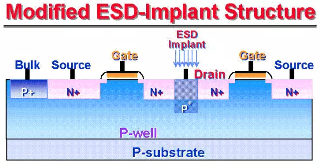
2) ESD implant of contact: punch a P+ boron under the hole of the N+ Drain of LDD device, and the depth should exceed the depth of the N+ Drain, so that the breakdown voltage of the original Drain can be reduced (8V-> 6V), so it can be conducted away from the drain before the sharp corner of LDD breaks down, thus protecting the breakdown of drain and Gate. Therefore, this design can keep the device size unchanged and the MOS structure unchanged, so there is no need to re-extract SPICE model. Of course, this kind of intelligence is used in the non-silicide process, otherwise you can't enter the implant contact.
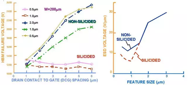
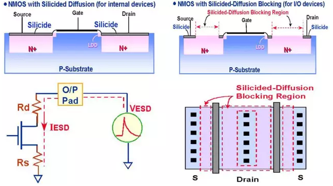
3) SAB (SAlicide Block): Generally, in order to reduce the interconnection capacitance of MOS, we will use silicide/SAlicide process. However, if the device works at the output, the load resistance of our device will become low, and the external ESD voltage will all be loaded between LDD and Gate structure, which is easy to break down and damage. Therefore, we usually use SAB(SAlicide Block) mask to block RPO in the output stage of MOS, and do not form silicide, which increases the cost of adding a photo layer, but the ESD voltage can be increased from 1kV to 4kV.
4) Series resistance method: This method does not need to add a mask, so it should be the cheapest. The principle is somewhat similar to the third (SAB) method of increasing resistance, so I deliberately connected a resistor (such as Rs_NW, or HiR, etc.) to him, thus reaching the SAB method.
2. ESD in design: This depends entirely on the efforts of designers. Some companies have already provided solution to customers in the design rules, and customers only need to follow the drawings, while others can only rely on customers' own designers if they don't. Many design rules state that this is just a guideline/reference, not a guarantee. Generally, the Gate/Source/Bulk are shorted together, and the Drain junction is connected to the I/O terminal to withstand the surge voltage of ESD. NMOS is called GGNMOS (Gate-Grounded NMOS), and PMOS is called GDPMOS (Gate-to-Drain PMOS).
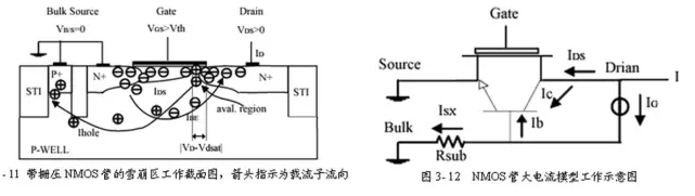
Take NMOS as an example, the principle is that the Gate is turned off, and the PN junction of Source/Bulk is originally short-circuited with zero bias. When there is a large voltage at the I/O terminal, the PN junction of drain/bulk is avalanche-broken. In an instant, there is a large current in bulk and a voltage difference between the substrate resistance causes the PN of Bulk/Source to be positively biased. Therefore, the parasitic lateral NPN transistor of this MOS enters the amplification area (the emitter junction is positively biased, and the collector junction is reversely biased), so it shows Snap-Back characteristics. PMOS is deduced in the same way.
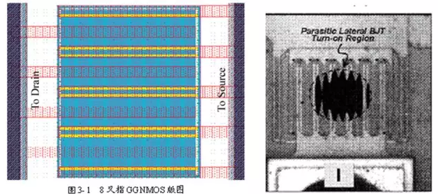
How to trigger? There must be a large enough substrate current, so it developed into the multi-finger cross-parallel structure which is now widely used. However, the main technical problem of this structure is that the base width increases and the amplification factor decreases, so the Snap-back is not easy to open. Moreover, with the increase of the number of fingers, it will be difficult to turn on each finger evenly, which is also the bottleneck of ESD design.
There are two little common sense to share with you about the ESD of Snap-back:
1) We can usually see better Snap-back characteristics of NMOS, but actually PMOS is difficult to have snap-back characteristics, and the ESD resistance of PMOS is generally better than that of NMOS. This reason is the same as HCI effect, mainly because electrons are generated when NMOS is broken down, and the mobility is very high, so Isub can easily make the Bulk/Source turn on positively, but PMOS is difficult.
2) Trigger voltage /Hold voltage: Trigger voltage is of course the first Knee-point of the previous snap-back, the breakdown voltage of parasitic BJT, and it should be between BVCEO and BVCBO. And the Hold voltage is to keep the Snap-back ON continuously, but it cannot enter the Latch-up state, otherwise it will enter the secondary breakdown (thermal breakdown) and be damaged. Another concept is the secondary breakdown current, that is, the sudden increase of I 2 * R heat after entering Latch-up causes the silicon to melt, and this is to limit the current, which can be achieved by controlling W/L or adding a current limiting and high resistance. The simplest and most commonly used method is to increase the distance between Drain and SAB (common practice of ESD rule).
3. Gate-Couple) ESD technology: As we just said, the bottleneck of ESD design of Multi-finger is the uniformity of turn-on. Suppose there are 10 fingers, but when ESD discharge occurs, these 10 Fingers may not be turned on at the same time (usually due to Breakdown). It is common that only 2-3 Fingers will turn on first. This is because the layout can't make the relative position and cable direction of each finger exactly the same. As soon as these 2~3 fingers are turned on, the ESD current will concentrate on these 2~3 fingers, while other fingers are still turned off, so its ESD protection capability is equivalent to that of only 2~3 fingers, instead of 10 fingers.That is the main reason why the component size has been made very large, but the ESD protection capability has not increased as expected. What should I do if the increased area can't bring about ESD enhancement as expected? Actually, it's very simple, that is, to reduce Vt1(Trigger voltage). By increasing the voltage at the gate, we make the substrate turn on first instead of breakdown and turn on in advance to generate substrate current. At this time, other fingers can also turn on and enter the conducting state, so that each finger can bear the ESD current, and really play a large-area ESD role.However, this kind of ESD design of GCNMOS has a disadvantage, that is, when the channel is turned on, the current is easy to cause gate oxide breakdown, so what he doesn't see is a good ESD design scheme. Moreover, the smaller the active area is, the greater the influence of gate voltage is, while the larger the active area is, the more difficult it is to turn on the snap-back, so it is difficult to grasp.
4. There is also a complex ESD protection circuit SCR: Silicon Controlled Rectifier (SCR), which is the PNPN structure of CMOS parasitic as we talked about before, which triggers to generate Snap-Back and Latch-up, and realizes the protection of the circuit through ON/OFF. You can review it. As long as those factor that inhibit LATCH-up in the last article can be made to happen, but they can only be applied to Layout, not Process, otherwise Latch-up will fail again.Finally, the knowledge of ESD design is too deep, so I'm just throwing a brick at FAB people to popularize it. Basically, ESD schemes are as follows: resistor divider, diode, MOS, parasitic BJT, SCR(PNPN structure) and other methods. Moreover, ESD is not only related to Design, but also to FAB's process, and the knowledge is too deep for me to understand.
Disclaimer: This article is reproduced from "Remember Honesty". This article only represents the author's personal views, not the views of Sacco Micro and the industry. It is only for reprinting and sharing to support the protection of intellectual property rights. Please indicate the original source and author when reprinting. If there is any infringement, please contact us to delete it.
Company Tel: +86-0755-83044319
Fax/fax:+86-0755-83975897
Email: 1615456225@qq.com
QQ: 3518641314 Manager Li
QQ: 332496225 Manager Qiu
Address: Room 809, Block C, Zhantao Technology Building, No.1079 Minzhi Avenue, Longhua New District, Shenzhen


