Service hotline
+86 0755-83044319

release time:2022-03-17Author source:SlkorBrowse:10301
Silicon carbide (SiC) is the main development direction of power semiconductor industry, which can significantly improve the utilization rate of electric energy when it is used to make power devices. In the foreseeable future, new energy vehicles will be the main application scenarios of silicon carbide power devices. As a pioneer in technology, Tesla has taken the lead in integrating all silicon carbide modules in Model 3, and other first-line car companies are also planning to expand the application of silicon carbide. With the decreasing manufacturing cost of silicon carbide devices and the gradual maturity of technology, the future of silicon carbide power device industry can be expected. [What is silicon carbide? Silicon carbide (SiC) is the third generation compound semiconductor material. The cornerstone of semiconductor industry is chips, and the core materials for making chips are divided into the first generation semiconductor materials (mostly high-purity silicon which is widely used at present), the second generation compound semiconductor materials (gallium arsenide and indium phosphide) and the third generation compound semiconductor materials (silicon carbide and gallium nitride) according to the historical process. Because of its superior physical properties: high bandgap (corresponding to high breakdown electric field and high power density), high electrical conductivity and high thermal conductivity, silicon carbide will be the most widely used basic material for semiconductor chips in the future. [Physical and Chemical Properties of Silicon Carbide]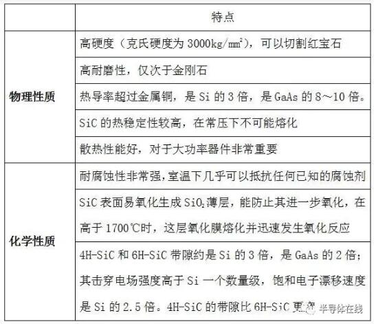 The main form of silicon carbide in semiconductor chips is substrate. Semiconductor chips can be divided into integrated circuits and discrete devices, but the basic structure of both integrated circuits and discrete devices can be divided into "substrate-epitaxial-device" structure. The main form of silicon carbide in semiconductors is as a substrate material.
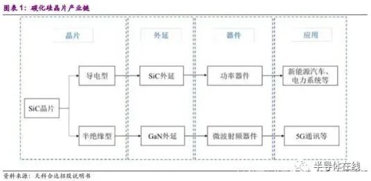 Silicon carbide wafer is a single crystal sheet formed by cutting, grinding, polishing and cleaning silicon carbide crystal. As a semiconductor substrate material, silicon carbide wafer can be made into silicon carbide-based power devices and microwave RF devices through epitaxial growth and device manufacturing, which is an important basic material for the development of the third generation semiconductor industry. According to the difference of resistivity, silicon carbide wafers can be divided into conductive type and semi-insulating type. Among them, conductive silicon carbide wafers are mainly used to manufacture high-temperature and high-voltage power devices, with a large market scale; Semi-insulating silicon carbide substrate is mainly used in microwave RF devices and other fields. With the accelerated construction of 5G communication network, the market demand has increased obviously.
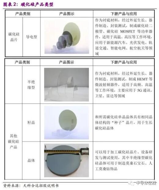 [Research on processing technology of silicon carbide] The hardness of SiC is second only to that of diamond, and it can be used as an abrasive for grinding tools such as grinding wheels. Therefore, diamond grinding wheels are mainly used for grinding, grinding and polishing, among which diamond grinding wheels have the highest efficiency and are an important means for processing SiC. However, SiC material not only has the characteristics of high hardness, but also its high brittleness and low fracture toughness make it easy to cause brittle fracture of the material in the grinding process, thus leaving a surface broken layer on the surface of the material, and causing serious surface and sub-surface damage, which affects the machining accuracy. Therefore, it is of great significance to deeply study the grinding mechanism and subsurface damage of SiC to improve the grinding efficiency and surface quality of SiC. 1. Grinding Mechanism of Hard and Brittle Materials Grind hard and brittle materials, and abrasives have rolling or micro-cutting effects on them. When abrasive particles act on the surface with bumps and cracks, with the progress of grinding, some abrasive particles are pressed into the workpiece under the action of grinding load, and the exposed tip is used to scratch the surface of the workpiece for micro-cutting. The other part of abrasive grains roll between the workpiece and the grinding disk to produce rolling action, which makes the surface of the workpiece form microcracks, and the crack extends to form brittle chips on the surface of the workpiece, thus achieving the purpose of surface removal. Because the tensile strength of hard and brittle materials is lower than the compressive strength, when the abrasive particles are loaded, microcracks will be generated at the maximum tensile stress on the surface of hard and brittle materials. When criss-crossing cracks extend and cross each other, the part surrounded by cracks will break and collapse into small pieces. This is the basic process of chip generation and surface formation when grinding hard and brittle materials. As silicon carbide is a kind of high-hardness brittle material, special grinding fluid is needed. The main technical difficulty of grinding silicon carbide lies in the accurate measurement and control of the thinning thickness of high-hardness material. After grinding, the surface of the wafer will be damaged, microcrack and residual stress, and the thinning of silicon carbide wafer will cause more warpage than that of silicon carbide wafer. 2. Research on the polishing processing of silicon carbide. At present, the polishing methods of silicon carbide mainly include mechanical polishing, magnetorheological polishing, chemical mechanical polishing (CMP), electrochemical polishing (ECMP), catalyst-assisted polishing or catalyst-assisted etching (CACP/CARE), tribochemical polishing (TCP) and plasma-assisted polishing (PAP). Chemical polishing (CMP) technology is an important means of semiconductor processing at present, and it is also the most effective technology to process the surface of single crystal silicon to atomic level. It is the only practical technology that can realize local and global planarization in the process of processing. The processing efficiency of CMP is mainly determined by the chemical reaction rate on the workpiece surface. By studying the influence of process parameters on the polishing rate of SiC materials, the results show that the rotation rate and polishing pressure have great influence; And the temperature and pH value of polishing solution have little influence. In order to improve the polishing rate of materials, the rotating speed should be increased as much as possible. Although increasing the polishing pressure can also improve the removal rate, it is easy to damage the polishing pad. At present, the polishing method of silicon carbide has the problems of low material removal rate and high cost, and there are no abrasive grinding and polishing, catalytic auxiliary processing and other processing methods. Because of the demanding conditions and complicated operation of the device, it is still in the laboratory, and it is unlikely to realize mass production. Silicon carbide was first discovered in meteorites in 1905, and now it mainly comes from artificial synthesis. Silicon carbide has many uses, and its industry span is wide. It can be used as engineering processing materials for monocrystalline silicon, polycrystalline silicon, potassium arsenide, Shi Ying crystal, etc., solar photovoltaic industry, semiconductor industry and piezoelectric crystal industry. [Process Flow of Silicon Carbide Processing] Silicon carbide wafers are made of high-purity silicon powder and high-purity carbon powder as raw materials, and silicon carbide crystals are grown by physical vapor transport (PVT), and then processed into silicon carbide wafers. ① raw material synthesis. High-purity silicon powder and high-purity carbon powder are mixed according to a certain proportion, and the silicon carbide particles are synthesized by reaction at a high temperature of over 2,000℃. After crushing, cleaning and other processes, high-purity silicon carbide micropowder raw materials meeting the requirements of crystal growth are prepared. ② Crystal growth. Using high-purity silicon carbide micropowder as raw material, silicon carbide crystal was grown by physical vapor transport (PVT) in a self-developed crystal growth furnace. Its growth principle is shown in the following figure:
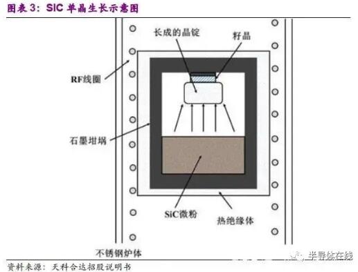 High-purity silicon carbide micropowder and seed crystal are respectively placed at the bottom and top of a cylindrical sealed graphite crucible in a single crystal growth furnace. The crucible is heated to over 2,000℃ by electromagnetic induction, and the temperature of the seed crystal is slightly lower than that of the lower micropowder, thus forming an axial temperature gradient in the crucible. Micro-powder of silicon carbide sublimates at high temperature to form gaseous substances such as Si2C, SiC2, Si, etc., and driven by temperature gradient, it reaches the seed crystal with lower temperature, and crystallizes on it to form cylindrical silicon carbide ingot. ③ Ingot processing. The obtained silicon carbide ingot is oriented by using an X-ray single crystal orienter, then ground flat and rolled, and processed into silicon carbide crystal with standard diameter. ④ Crystal cutting. Use multi-wire cutting equipment to cut the silicon carbide crystal into thin slices with a thickness of no more than 1mm. ⑤ wafer grinding. Grinding the wafer to the required flatness and roughness by diamond grinding fluid with different particle sizes. ⑥ wafer polishing. A silicon carbide polishing wafer with no surface damage is obtained by mechanical polishing and chemical mechanical polishing. ⑦ wafer inspection. Using optical microscope, X-ray diffractometer, atomic force microscope, non-contact resistivity tester, surface flatness tester, surface defect comprehensive tester and other instruments and equipment, various parameters such as microtubule density, crystal quality, surface roughness, resistivity, warpage, curvature, thickness change, surface scratch of silicon carbide wafer were detected, and the quality grade of the wafer was judged accordingly. ⑧ Wafer cleaning. Cleaning the silicon carbide polishing sheet with cleaning agent and pure water to remove the residual surface contaminants such as polishing solution on the polishing sheet, and then blowing and spinning the wafer by ultra-high purity nitrogen and a spin dryer; The wafer is packaged in a clean wafer box in an ultra-clean room to form a silicon carbide wafer which can be opened and used immediately downstream. The larger the wafer size, the more difficult it is to grow and process the corresponding crystal, while the higher the manufacturing efficiency of downstream devices, the lower the unit cost. At present, international silicon carbide wafer manufacturers mainly provide 4-inch to 6-inch silicon carbide wafers, and international leading enterprises such as CREE and II-VI have started to invest in the construction of 8-inch silicon carbide wafer production lines. [Situation of Silicon Carbide Industry]01. Silicon carbide (SiC) is an ideal material for high-power devices. Silicon is the first generation basic material in the semiconductor industry. At present, more than 95% of integrated circuit components in the world are made of silicon. At present, with the development of electric vehicles, 5G and other applications, the demand for high-power, high-voltage and high-frequency devices is increasing rapidly. When the voltage is greater than 900V, the short board of silicon-based power MOSFET and IGBT will be exposed, which will be limited in many aspects such as conversion efficiency, switching frequency and working temperature. Silicon carbide (SiC) is widely used in high temperature, high voltage, high frequency, high power electronic devices, aerospace, and other extreme environments because of its wide bandgap (3 times of Si), high thermal conductivity (3.3 times of Si or 10 times of GaAs), high electron saturation migration rate (2.5 times of Si) and high breakdown electric field (5 times of Si or GaAs). Silicon carbide is made by smelting quartz sand, petroleum coke (or coal coke), sawdust (salt is needed when green silicon carbide is produced) and other raw materials in a resistance furnace at high temperature. 02. Advantages of SiC power semiconductor devices The third generation semiconductor, also known as wide bandgap semiconductor because of its physical structure, is mainly represented by gallium nitride and silicon carbide. Its semiconductor performance characteristics are different from those of the first generation silicon and the second generation gallium arsenide, which makes it have the advantages of high bandgap, high thermal conductivity, high breakdown field strength and high electron saturation drift rate. Thereby being able to develop miniaturized power semiconductor devices which are more suitable for harsh conditions such as high temperature, high power, high voltage, high frequency and radiation resistance, and effectively breaking through the physical limits of traditional silicon-based power semiconductor devices and their materials.
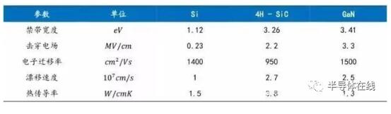
At present, the main preparation process of SiC substrate is roughly divided into two steps: the first step is that SiC powder is sublimated at high temperature in a single crystal furnace and then SiC ingot is formed in the single crystal furnace; Secondly, rough machining, cutting, grinding and polishing the SiC ingot to obtain a transparent or translucent SiC wafer (i.e. SiC substrate) with no damage layer and low roughness.

Technical evolution direction: in terms of devices, high withstand voltage devices above 3.3kv are being developed, and trench design is introduced to improve device performance and reliability; In terms of packaging, the packaging process will be optimized to give full play to the advantages of high temperature resistance of silicon carbide.


Site Map | 萨科微 | 金航标 | Slkor | Kinghelm
RU | FR | DE | IT | ES | PT | JA | KO | AR | TR | TH | MS | VI | MG | FA | ZH-TW | HR | BG | SD| GD | SN | SM | PS | LB | KY | KU | HAW | CO | AM | UZ | TG | SU | ST | ML | KK | NY | ZU | YO | TE | TA | SO| PA| NE | MN | MI | LA | LO | KM | KN
| JW | IG | HMN | HA | EO | CEB | BS | BN | UR | HT | KA | EU | AZ | HY | YI |MK | IS | BE | CY | GA | SW | SV | AF | FA | TR | TH | MT | HU | GL | ET | NL | DA | CS | FI | EL | HI | NO | PL | RO | CA | TL | IW | LV | ID | LT | SR | SQ | SL | UK
Copyright ©2015-2025 Shenzhen Slkor Micro Semicon Co., Ltd
