Those who engage in power electronics may be familiar with IGBT. The full name is Insulated Gate Bipolar Transistor, which is a composite fully-controlled power semiconductor device composed of MOS (Insulated Gate Field Effect Transistor) and BJT (Bipolar Transistor). It is commonly known as the "CPU" of power electronic devices. Through a gate control signal of more than ten volts, It can realize the control of kV voltage and kA current. As a national strategic emerging industry, it is widely used in rail transit, smart grid, industrial energy saving, electric vehicles and new energy equipment.But do you really know IGBT? Today, let's discuss the turn-off process of IGBT. Before we start, let's throw a question. You can consider it. Figure 1 shows the relationship between the turn-off gate resistance of IGBT and the voltage spike: 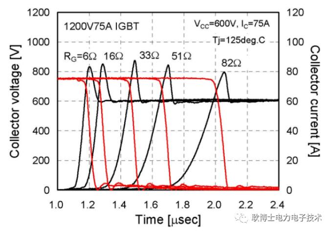 Figure 1. Relationship between IGBT turn-off overvoltage and gate resistance [1]When the gate off resistance of IGBT is increased, the voltage spike will increase? What kind of ghost is this? Is it different from what we thought?Let's look at the relationship between the turn-off resistance and the turn-off loss of IGBT. It can be seen from Figure 2 that the turn-off resistance of IGBT has little effect on the turn-off loss.
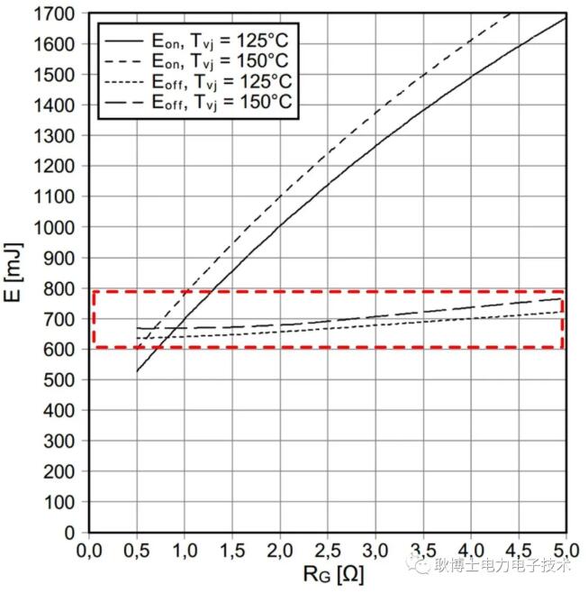
From the above two pictures, it seems that it is not ideal to influence the turn-off characteristics of IGBT through gate resistance. However, this is the case, so is there no solution? There must be some methods, first sell a imprison son, and then we'll talk about it later!Today, let's briefly talk about the shutdown process of IGBT, and analyze the causes of the above phenomenon from the root.To understand the turn-off process of IGBT, it is necessary to briefly review the working principle of IGBT. As mentioned earlier, IGBT is a power device composed of MOS and BJT. Figure 1 shows the internal structure and equivalent circuit of NPT IGBT. We all know that IGBT is a bipolar device, that is, both electrons and holes participate in conduction. AssumIng that the electron current flowing through MOS is in and the hole current flowing through pnp transistor is Ip, the collector current IC flowing through IGBT is in+IP.
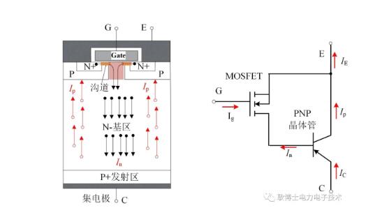
AccordIng to the working principle of the transistor, the following relationship exists between the collector current Ip and the base current in of the PNP transistor:
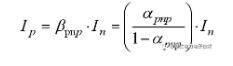
βpnp is the common emitter current amplification factor of the transistor, and αpnp is the common base current amplification factor of the transistor. It should be noted that the PNP transistor on the collector side of IGBT is only equivalent to PNP transistor in structure, which is far from the transistor actually used for current amplification in performance [3]. The real transistor can amplify the current, that is, Ip>>In, while for IGBT, the electron current In is basically equal to the hole current Ip.After talking about transistors, let's talk about MOS. We all know that MOS is a voltage-controlled device. The channel current In of MOS has the following relationship with the gate voltage in the switching process: 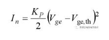 In this formula, Kp is the coefficient related to the device structure and carrier characteristics, and Vge,th are the threshold voltages.At this point, it may be a little clear to everyone that what we control the gate voltage of IGBT is actually the internal MOS, which is directly affected by the electron current In, while the hole current Ip is not directly related to the gate voltage Vge.Back to the topic, let's take a look at the turn-off process of IGBT. Usually, the turn-off process of IGBT can be divided into five stages according to its external characteristics, as shown in the following figure:
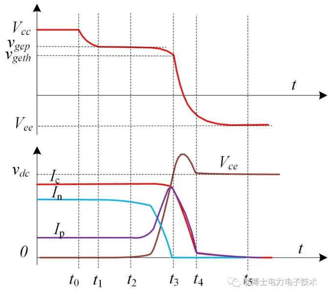
图4.
IGBT关断外特性
Stage 1(t0-t1): the gate capacitor discharges, and the gate voltage drops exponentially to the Maitreya platform voltage Vgep.
Stage 2(t1-t2): In the stage of Maitreya platform, the gate voltage is basically unchanged, and the Vgep voltage depends on the load current. The gate current charges the Maitreya capacitor, and the collector voltage rises slightly.
Stage 3(t2-t3): In the stage of rising collector voltage, the collector voltage Vce of IGBT quickly rises to the bus voltage. At the same time, the gate voltage drops from the Maitreya platform Vgep to the threshold voltage Vge,th, and the gate is completely turned off.
Stage 4(t3-t4): In the stage of collector current decreasing, the collector voltage of IGBT has risen to the bus voltage Vdc, and the diode corresponding to IGBT enters the forward conduction stage, and the load current is quickly transferred from IGBT to diode. The current of Ic drops rapidly to the trailing current, and the collector voltage has a certain voltage overshoot due to the existence of stray inductance.
Stage 5(t4-t5): Trailing current process, the speed of current decline in this stage is mainly determined by the carrier lifetime of the device.
Some people may ask why the gate is turned off when the current begins to drop. Many papers show that when the collector current of IGBT drops to 0, the gate will turn off. These figures have no problem in simply understanding the switching characteristics of IGBT. Strictly speaking, there are some problems, but let's not get too entangled. In fact, it is difficult for us to test when the gate of IGBT is turned off, because we are not studying semiconductors after all, and we don't know many parameters!
The following describes the turn-off process of IGBT from the internal mechanism level:
First, look at the distribution of internal carriers before the IGBT is turned off. Fig. 5 corresponds to the distribution of internal carriers in the IGBT before t0 in fig. 4, that is, in the on state. Here, we mainly discuss the carrier distribution in the N- base region, because the switching characteristics of IGBT are mainly affected by the carriers in the N- base region. On-state, the N- base region is full of electrons and holes, so this region can also be called Carrier Storage Region (CSR) or Plasma. During the on-state process, the electron current and hole current in the base region of IGBT are approximately 3: 1, mainly because the mobility of electrons is three times that of holes under the same conditions [4].
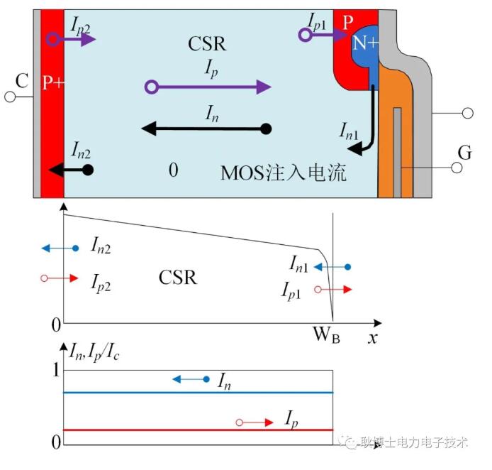
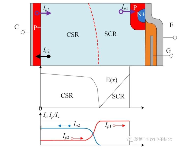
Carrier distribution before time 0 When a zero or negative bias voltage is applied to the gate of IGBT, the device enters the shutdown process. Firstly, with the decrease of gate voltage, the electron current injected from the N+ source region to the N- base region through the MOS channel gradually decreases, while the external collector current remains unchanged under the influence of the load inductance, so the electron current and hole current inside the IGBT module will deviate from their original equilibrium state. Fig. 3 depicts the change of carriers in the N- base region of IGBT at this stage, corresponding to the carrier distribution in t0-t3 in fig. 4, in which a large number of electron and hole pairs still exist in CSR region on the left side of the N- base region. On the right side of the N- base region, there is a Space Charge Region (SCR), which has no residual carriers and can also be called depletion layer. During the turn-off of IGBT, this region carries voltage, and the electron current in SCR region gradually decreases, while the hole current gradually increases.
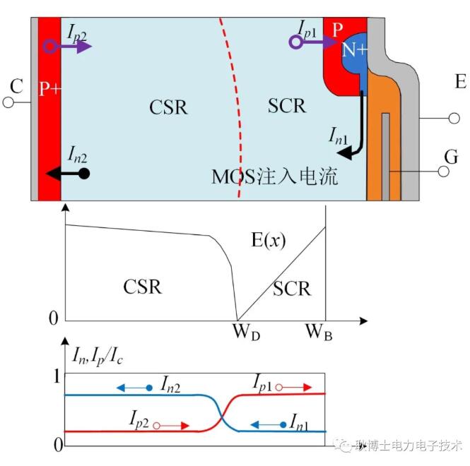
Carrier distribution in 0-t3 period
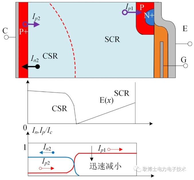
When the gate voltage of IGBT continues to decrease to the threshold voltage Vgeth, the internal MOS conduction channel is completely turned off, and In1 is 0, which cuts off the base current of PNP transistor. The emitter of PNP transistor will no longer inject holes into the N- base region. Fig. 7 corresponds to t3 of IGBT's off-characteristic. At this time, the electron current in the space charge region is zero, and the load current is completely maintained by the hole current Ip1, while the electrons and holes in CSR region still exist.
3-hour carrier distribution
When the collector voltage Vce of IGBT rises to the bus voltage, the collector current drops rapidly, and the drop rate of IC is determined by the characteristics of the device itself, which will no longer be controlled by the gate. Fig. 8 corresponds to t3-t4 in fig. 4. After the completion of this stage, there are still a few carriers left in CSR area, and the elimination of the remaining carriers is mainly determined by their recombination rate, which appears as trailing current externally.
Carrier distribution in 3-t4 period
At this point, you may understand that whether the current drop rate of IGBT collector can be controlled by the gate depends on whether the electron current injected by MOS channel still plays a role in the IGBT current drop stage. Here we can use the formula to describe the turn-off decline rate of IGBT: 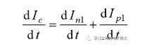 It is not difficult to find out from the formula that In1 must have a certain right to speak in order to control the falling slope of collector current when it is turned off. How can we increase the proportion of MOS channel electron current?
There are two methods, one is to slow down the turn-off speed of IGBT, and the other is to inject electron current into the gate. At present, both methods have good applications in IGBT gate drive. What are the ways to slow down the shutdown speed? Of course, it is possible to increase the resistance, but the turn-off delay or loss is very large, which is not worth the loss; The other method is to adopt active drive technology, and take measures to slow down the turn-off speed of IGBT only when the current of IGBT drops. This method can achieve a good compromise between switching delay, overvoltage and loss. Domestic Feishide digital driver has this function, so those who are interested can learn about it (it's not advertising here, it's purely technical exchange)! Then how to inject current into the gate? This is what we often call collector voltage active clamping technology.
Disclaimer: This article is reproduced from "Automotive Semiconductor Intelligence Bureau". This article only represents the author's personal views, and does not represent the views of Sacco Micro and the industry. It is only for reprinting and sharing to support the protection of intellectual property rights. Please indicate the original source and author when reprinting. If there is any infringement, please contact us to delete it.
Company Tel: +86-0755-83044319
Fax/fax:+86-0755-83975897
Email: 1615456225@qq.com
QQ: 3518641314 Manager Li
QQ: 332496225 Manager Qiu
Address: Room 809, Block C, Zhantao Technology Building, No.1079 Minzhi Avenue, Longhua New District, Shenzhen


