Service hotline
+86 0755-83044319
release time:2022-03-17Author source:SlkorBrowse:11387
Phase-locked loop (PLL) is a feedback system, in which a voltage-controlled oscillator (VCO) and a phase comparator are connected to each other, so that the oscillator can maintain a constant phase angle with respect to a reference signal. What problems have you encountered in using PLL? Our engineers sorted out the 11 most common problems in PLL chip interface, and share them with you here!
Waveform: sine wave or square wave.
Power: meet the requirements of reference input sensitivity.
Stability: TCXO is usually used, and the stability requirement is < 2 ppm. Here are some reference stability indexes and phase noise indexes.
Frequency range: PLL products provided by ADI can also work below the minimum reference input frequency, provided that the conversion rate of the input signal meets the given requirements.
In the design of PLL frequency synthesizer, we recommend using temperature compensated crystal oscillator (TCXO). When using VCXO when fine-tuning reference is needed, it should be noted that VCXO has a small sensitivity, such as 100Hz/V, so the bandwidth of the loop filter should not be large (such as 200Hz), otherwise the capacitance of the filter will be large and the resistance will be small. Ordinary crystal oscillator is not recommended for high-precision frequency design because of its poor temperature stability.
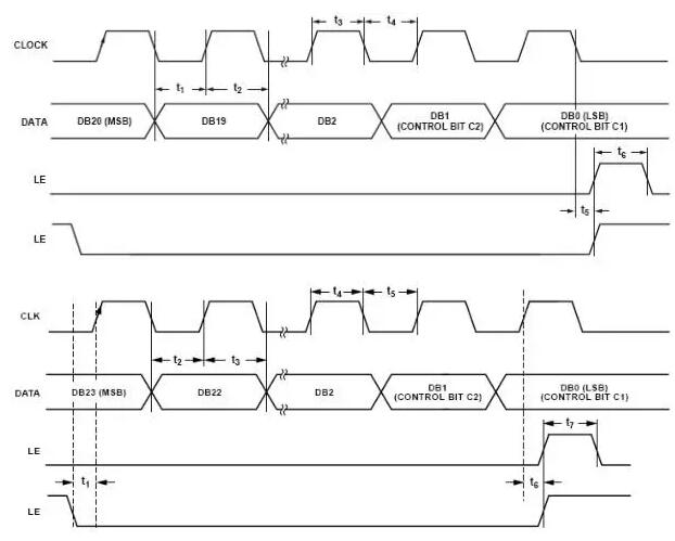
All of ADI's PLL product control interfaces are three-wire serial control interfaces, as shown in Figure 1. It should be noted that in the PLL products of ADI, most of the timing diagrams are shown in the upper diagram of Figure 1, which is wrong, and the correct timing diagram is shown in the lower diagram of Figure 1. The rising edge of LE should be aligned with the rising edge of Clock, not the falling edge of Clock.

图 1. PLL 频率合成器的串行控制接口(3 Wire Serial Interface)
The control interface consists of CLOCK, DATA data and load enable LE. The falling edge of the load enable LE provides synchronization of the initial serial data. The serial data is first shifted to the shift register of PLL frequency synthesizer, and then the corresponding internal register is updated on the rising edge of LE. Note that there are two control methods of LE in the timing diagram.
SPI control interface is 3V/3.3V CMOS level. In addition, it should be noted that when the register of PLL chip is written, it needs to be written in a certain order. Please refer to the description in the chip data for details. Especially, when operating the register of ADF4360, pay attention to a certain delay between the write control register and the N counter.
The control signal can be generated by MCU, DSP or FPGA. The generated clock and data must be clean and have little overshoot. When using FPGA, it is necessary to avoid competition and risk, and to prevent burr. If burrs cannot be avoided, a 10~47pF capacitor can be connected in parallel between the data line and the clock line to absorb these burrs.
Generally, the signals controlling PLL include CE, LE, CLK and DATA. And the CLK and DATA signals can be shared, that is, the IO ports of two mcus are occupied, and the LE signal is used to control which PLL chip to operate on. Multiple LE signals can also share the IO port of one MCU. At this time, CE signal is needed to control the power-on and power-off of the chip.
Adisimplv3.3 frees application engineers from complicated mathematical calculations. As long as we input several key parameters for setting the loop filter, ADIsimPLL can automatically calculate the values of the filter components we need. These parameters include phase detection frequency PFD, charge pump current Icp, loop bandwidth BW, phase margin, VCO control sensitivity Kv, filter form (active or passive, order). The calculated result is often not the value of the components that we can buy in the market, just choose the one closest to the components.
Usually, the bandwidth of the loop is set to 1/10 or 1/20 of the phase detection frequency.
The phase margin is set to 45 degrees.
Passive filters are preferred.
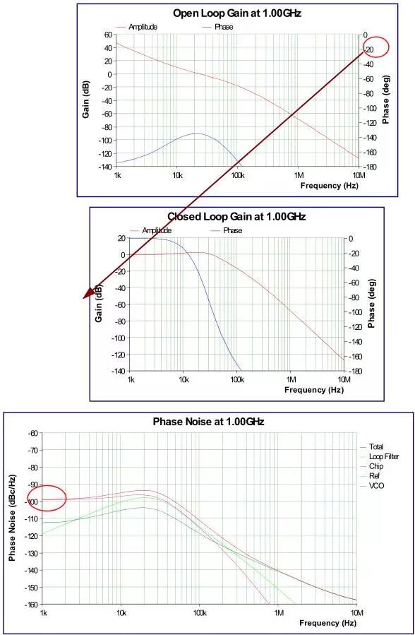
Relationship between open-loop gain and closed-loop gain of filter and phase noise figure. The corner frequency of the closed-loop gain is the loop bandwidth. On the phase noise diagram, this point corresponds to the turning frequency of the phase noise curve. If the noise of the designed PLL is too loud, the corner frequency seen by the spectrum analyzer will be larger than the set loop bandwidth.

Active filter introduces noise because of amplifier, so the phase noise performance of PLL with active filter will be worse than that of PLL with passive filter. Therefore, we try to choose passive filters in the design. Among them, the third-order passive filter is the most commonly used structure. Generally, the charge pump voltage Vp of PLL frequency synthesizer is 5V or slightly higher, and the maximum control voltage of charge pump current integrated by loop filter is lower than Vp or close to Vp.
If the control voltage of VCO/VCXO is within this range, the passive filter is fully capable; If the control voltage of VCO/VCXO exceeds Vp or is very close to Vp, an active filter is needed. While filtering the loop error signal, it also provides a certain gain, so as to adjust the VCO/VCXO control voltage to a suitable range.
So how do you choose the amplifier of active filter? This kind of application is mainly concerned about the technical indicators:
Low Offset Voltage) [usually less than 500uV]
If it is powered by a single power supply, Rail-to-Rail output amplifier should be considered.
When choosing VCO, try to choose the control voltage corresponding to the output frequency of VCO at the midpoint of the available tuning voltage range. Choosing VCO with low control voltage can simplify PLL design.
The output of VCO is distributed by a simple resistor distribution network. From the output of VCO, the impedance of the resistor network is 18+(18+50)/(18+50) = 52 ohm. Matching with the output impedance of VCO. ABC three-point power relationship in the following figure. The power of point B and C is 6dB less than that of point A.
The following diagram shows the output matching circuit of ADF4360-7 when the output frequency is 850MHz~950MHz. Note that this example matches the load of 50 ohms. If the load is 75 ohms, the matching circuit does not need to be changed. The output stage of ADF4360-7 is a current source, and small changes in the load value will not have a great impact, but it should be noted that the loads at the differential output terminals should be equal.
Under the following conditions, the polarity of the charge pump is positive.
The loop filter is a passive filter, and the control sensitivity of VCO is positive (that is, the output frequency increases with the increase of control voltage).
Under the following conditions, the polarity of the charge pump is negative.
The loop filter is an active filter, and the amplification link is inverse amplification;
The control sensitivity of VCO is positive.The loop filter is passive, and the control sensitivity of VCO is negative.
PLL frequency division application, the filter is passive. That is, the reference signal is directly fed back to the frequency division input terminal of RF, and the VCO is fed back to the reference input.
PLL lock indication is divided into analog lock indication and digital lock indication.

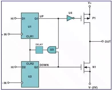
鉴相器和电荷泵原理图
Digital lock indication:
When the input of PFD continuously detects that the phase error is less than 15ns for 3(5) times, the PLL will give a digital locking indication.

Operating frequency range of digital locking indication: usually 5kHz~50MHz. At a lower PFD frequency, the leakage current will trigger the lock indication circuit; At higher frequencies, the time margin of 15ns is no longer suitable. Outside the working frequency range of digital locking indication, analog locking indication is recommended.
Analog lock indication:
The pulse train obtained by exclusive or processing the Up pulse and the Down pulse at the input of the charge pump. Therefore, when locked, the output of the lock indicating circuit is a high-level signal with a narrow negative pulse train. The figure shows a typical analog locking indication output (when the output of MUXOUT is added with a pull-out resistor alone).
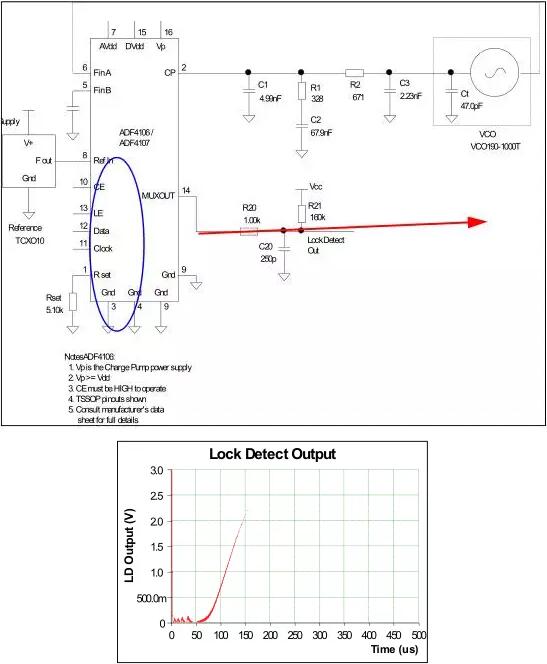
The output stage of analog locking indicator is N-channel open-drain structure, which requires an external pull-up resistor, which is usually 10KOhm~160kohm. We can get a flat high-level output through an integrating circuit (low-pass filter), such as the blue frame circuit shown in the figure.

A condition of false locking:
The reference signal REFIN signal is lost. When REFIN signal is disconnected from PLL frequency synthesizer, PLL will obviously lose lock; However, for the PLL of ADF41xx series, the digital lock indication is to check whether it is locked with REFIN clock. If the PLL has been locked before and the REFIN clock is suddenly lost, the PLL will continue to display the locked state. The solution is to use the analog lock indication.
The reason why PLL often loses lock when VCXO replaces VCO. Take ADF4001 as an example. The input impedance of VCXO is usually small (relative to VCO), about 100kohm. In this way, the current required by VCXO must be provided by PLL. PFD=2MHz, Icp=1.25mA, Vtune=4V, VCXO input impedance = 100khm, VCXO control port current =4/100k=40uA. At the input of PFD, it is used to offset the static phase error required by the input current of VCXO.
16ns>15ns, so the digital lock indication is low.
Solution 1, use analog lock indication.
Solution 2: Use higher charge pump current to reduce static phase error. Increase the capacitance of loop filter to slow the discharge.
Frequency index: It can work at the frequency lower than the minimum RF input signal, provided that the Slew Rate of RF signal meets the requirements.
For example, the ADF4106 data sheet specifies that the minimum RF input signal is 500MHz and the power is -10dBm, which corresponds to a peak-to-peak value of 200mV and slew rate=314V/us. If your input signal frequency is lower than 500MHz, but the power meets the requirements, and the slew rate is greater than 314V/us, then the ADF4106 can also work normally. Generally, the conversion rate of LVDS drivers can easily reach 1000V/us.

PLL power supply and charge pump power supply are required to have good decoupling, while the charge pump power supply has more stringent requirements. The concrete implementation is as follows:
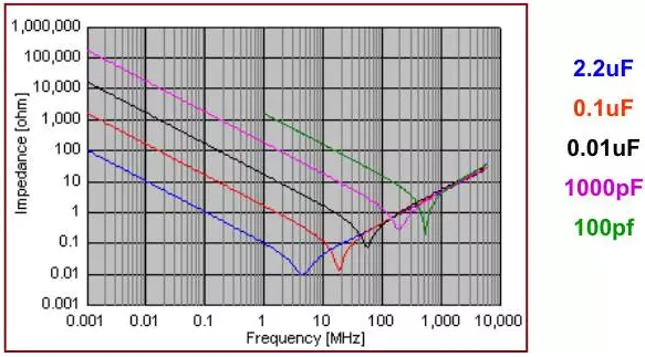
0.1uF, 0.01uF and 100pF capacitors are placed at the power supply pin in turn. Filter the interference on the power line to the maximum extent. The equivalent series resistance of a large capacitor is often large, and the filtering effect of high-frequency noise is poor, so the suppression of high-frequency noise requires a capacitor with small capacitance. As can be seen from the figure below, with the increase of frequency, after a certain turning frequency, the capacitor begins to show the characteristics of inductance. The turning frequency is often different for different capacitance values. The larger the capacitance, the lower the turning frequency, and the worse its ability to filter out high-frequency signals.

In addition, connecting a small resistor (18ohm) in series with the power line is also a common method to isolate noise.
The center frequency of VCO is determined by the following three factors.
1)Capacitor C VCO of VCO
2) Inductance L BW introduced by Bond Wires inside the chip
3) external inductor L EXT. namely

The first two terms are determined by the device, so that the output center frequency of VCO can be obtained if an external inductor is given. The control sensitivity of VCO is given in the corresponding data sheet. As an example, the following figure shows the integrated VCO characteristics of ADF4360-7.
ADF4360-7 VCO 的灵敏度与外置电感的关系
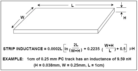
The choice of inductance, it is best to choose high Q value. Coilcraft company is a good choice. The common inductors on the market are basically above 1nH. Smaller inductors can be made of PCB wires. Here is a simple formula for calculating the inductance of PCB leads, as shown in the following figure.

导线电感的模型
Disclaimer: This article is reproduced from "Core Express". This article only represents the author's personal views, and does not represent the views of Sacco Micro and the industry. It is only for reprinting and sharing to support the protection of intellectual property rights. Please indicate the original source and author when reprinting. If there is any infringement, please contact us to delete it.



Site Map | 萨科微 | 金航标 | Slkor | Kinghelm
RU | FR | DE | IT | ES | PT | JA | KO | AR | TR | TH | MS | VI | MG | FA | ZH-TW | HR | BG | SD| GD | SN | SM | PS | LB | KY | KU | HAW | CO | AM | UZ | TG | SU | ST | ML | KK | NY | ZU | YO | TE | TA | SO| PA| NE | MN | MI | LA | LO | KM | KN
| JW | IG | HMN | HA | EO | CEB | BS | BN | UR | HT | KA | EU | AZ | HY | YI |MK | IS | BE | CY | GA | SW | SV | AF | FA | TR | TH | MT | HU | GL | ET | NL | DA | CS | FI | EL | HI | NO | PL | RO | CA | TL | IW | LV | ID | LT | SR | SQ | SL | UK
Copyright ©2015-2025 Shenzhen Slkor Micro Semicon Co., Ltd