Service hotline
+86 0755-83044319

release time:2022-03-17Author source:SlkorBrowse:10776
This week, we started the first part of the embedded system introductory course-PCB design. The objectives of our course are set as follows:
Master a useful programming language in the future
Deeply understand the composition and core points of "embedded system"
Cultivate ways to quickly use new products and solve unknown problems.
Cultivate the ability to draw inferences from others and draw inferences from others.
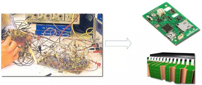
Understand the hardware and software components of embedded system from the system level. Hardware composition needs to start with designing PCB by yourself. Most beginners of embedded systems have no experience in hardware design, so they need to have some basic knowledge of PCB before starting formal PCB design.
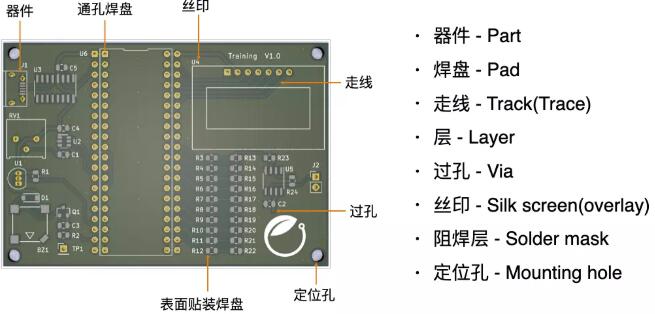
The function of PCB is to place all the devices in the circuit design on a board, and to be able to talk about the correct electrical connection of these devices.
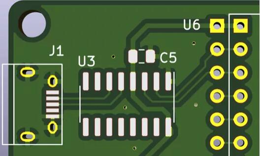
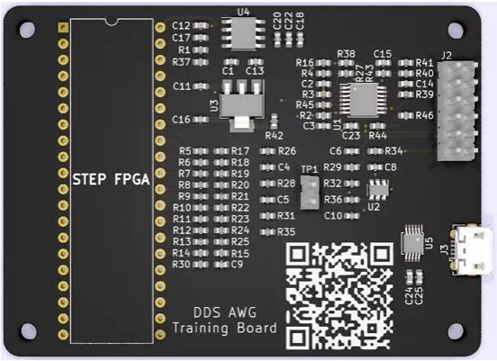
Many students have seen PCB, because any electronic product will have PCB, but what are the basic elements of PCB? The following figure gives a simple summary.
Many students have seen PCB, because any electronic product will have PCB, but what are the basic elements of PCB? The following figure gives a simple summary.
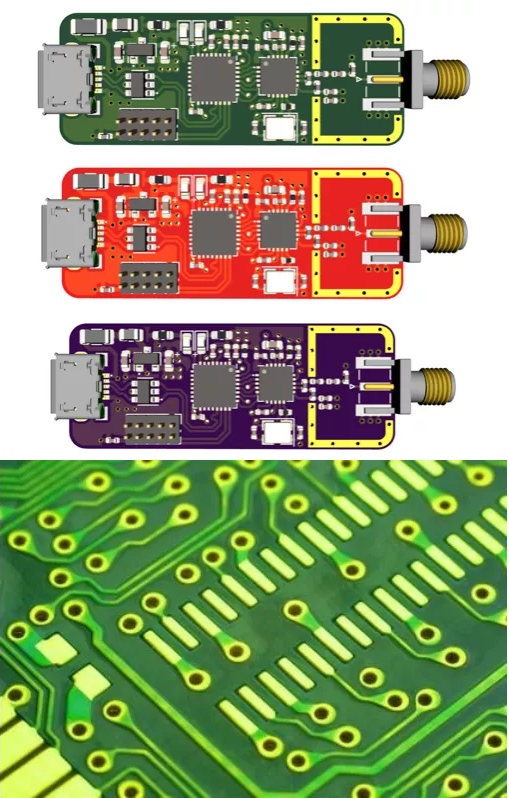
Many of the devices we use have different packages for the same model, so choose the appropriate ones according to your own needs.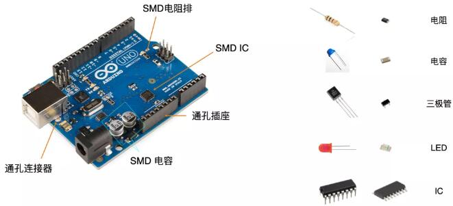
Surface mount SMD devices are widely used because of their small size, low cost, easy circuit board processing/production, higher board density and faster speed:
The connection between components and PCB board is realized by PAD-PAD. You can think of pad as the contact point where our toes touch the ground. The so-called Footprint of PCB package can be regarded as our footprints on the ground.
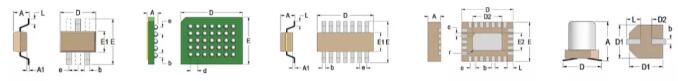
As the components are packaged in through-hole packages and SMD packages, there are many shapes of pads.
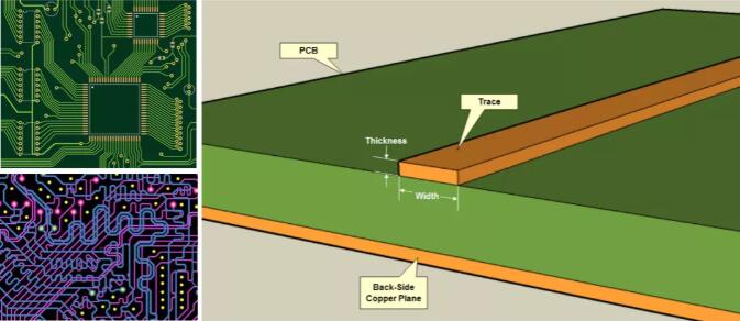
The electrical connection between the pins on the PCB is called Trace or Track in PCB design tools, which is equivalent to the path in our life and corresponds to the wires on the schematic diagram.
Just like the paths we see on the map, the connections on the schematic diagram are idealized, with no distance, thickness and impedance, and there is no relationship between the connections. However, on the actual PCB, the length and thickness of these "paths" will have an impact on the signal transmission, and the lines will also have an impact on each other. The gap between ideal and reality can be explained by electromagnetic field theory.
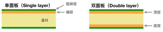
What do we mean by single-panel, single-layer board, double-panel, double-layer board and four-layer board? The concept of "layer" is different in PCB design tools.
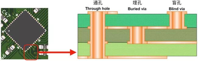
In our life, we will use stairs to connect different floors, from one side of the road to the other through overpasses and underpasses. In the process of PCB routing, we will also use Via holes for cross-floor routing. Why do you use Via as little as possible during high-speed signal transmission? Well-known conclusion-don't run at right angles, isn't via hole running at right angles? Can't you use vias?
Silk screen, like house numbers and road signs in our life, also plays a role of indication on PCB. It is necessary but not messy. How to put it can also reflect an engineer's design experience and aesthetics:
We often see boards of different colors. What's the difference? Actually, it is a layer of solder resist paint used for Mask, which not only makes your board look good, but more importantly, it is like the mask we wear to protect the pads and wires on our PCB.
I'm used to putting mounting holes with a diameter of 3mm at the four corners of each PCB. Why? It is not only used to fix and install the board, but also can help us keep a certain distance from the cluttered desktop when debugging, to prevent being short-circuited by the wires on the desk, and to facilitate the measurement of the bottom signal.
Disclaimer: This article is reproduced from "Electronic Forest". This article only represents the author's personal views, and does not represent the views of Sacco Micro and the industry. It is only for reprinting and sharing to support the protection of intellectual property rights. Please indicate the original source and author when reprinting. If there is any infringement, please contact us to delete it.
Company Tel: +86-0755-83044319
Fax/fax:+86-0755-83975897
Email: 1615456225@qq.com
QQ: 3518641314 Manager Li
QQ: 332496225 Manager Qiu
Address: Room 809, Block C, Zhantao Technology Building, No.1079 Minzhi Avenue, Longhua New District, Shenzhen


Site Map | 萨科微 | 金航标 | Slkor | Kinghelm
RU | FR | DE | IT | ES | PT | JA | KO | AR | TR | TH | MS | VI | MG | FA | ZH-TW | HR | BG | SD| GD | SN | SM | PS | LB | KY | KU | HAW | CO | AM | UZ | TG | SU | ST | ML | KK | NY | ZU | YO | TE | TA | SO| PA| NE | MN | MI | LA | LO | KM | KN
| JW | IG | HMN | HA | EO | CEB | BS | BN | UR | HT | KA | EU | AZ | HY | YI |MK | IS | BE | CY | GA | SW | SV | AF | FA | TR | TH | MT | HU | GL | ET | NL | DA | CS | FI | EL | HI | NO | PL | RO | CA | TL | IW | LV | ID | LT | SR | SQ | SL | UK
Copyright ©2015-2025 Shenzhen Slkor Micro Semicon Co., Ltd
