Service hotline
+86 0755-83044319

release time:2022-03-17Author source:SlkorBrowse:10403
一.summary
In the assembly and welding of electronic products, the phenomenon of virtual welding has always been a most prominent problem that puzzles the reliability of solder joints, especially in high-density assembly and lead-free welding. In history, there are numerous cases in which electronic products fail due to virtual welding, which leads to accidents.
The phenomenon of virtual welding has complex causes, wide influence and great concealment, which leads to great losses. In practical work, in order to find a virtual solder joint, it often takes a lot of manpower and material resources, and the radical measures involve a wide range, so it is not easy to establish a long-term and stable solution. Therefore, the problem of virtual soldering has always been the focus of the electronic industry.
In modern electronic assembly welding, cold welding is a high-incidence defect in reflow soldering of BGA and CSP packaged chips with pitch ≤ 0.5 mm. In this kind of devices, due to the concealment of welding parts, it is difficult to transfer heat to the solder joints of solder balls, so the probability of cold welding is even higher than that of virtual welding.
However, because cold welding is very similar to virtual welding in defect phenomenon, it is often misjudged as virtual welding and covered up. When dealing with the problem of circuit function failure originally caused by cold welding, it is often treated by virtual welding, and the result is that it takes a lot of effort and just has little effect.
The quality consequences caused by cold welding and virtual welding are similar in form, but the formation mechanism is just different. It is difficult to distinguish virtual welding from cold welding without visual image discrimination. It is difficult to fully expose them in the production process, and it often takes users a period of time (ranging from a few days to a few months or even a year) before they are fully exposed. Therefore, not only the impact is extremely bad, but also the consequences are serious.
What is cold welding in this article? The mechanism of cold welding, the criterion of cold welding spot, the analysis of defect degree of cold welding spot, the causes and countermeasures of cold welding, and the similarities and differences between virtual welding and cold welding.
二.cold welding
1.Definition and characteristics
The minimum required wetting temperature is not reached between the solder and the base metal during welding; Or the phenomenon caused by incomplete metallurgical reaction, although local wetting occurs, can be defined as cold welding, as shown in Figure 1.
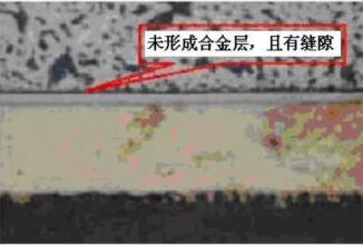
Figure 1 Microscopic characteristics of cold welding
It shows that there is no problem in solderability of PCB and components, and the fundamental reason for this phenomenon is that the soldering temperature is not suitable.
2.mechanism
The main reason for cold welding is that the heat supply is insufficient during welding, and the welding temperature does not reach the wetting temperature of solder, so IMC is not formed on the bonding interface or IMC is too thin, as shown in Figure 2. In some cases, the world
There are cracks in Shanghai, as shown in Figure 3.
图 2 未形成 IMC
picture 3 Mixed with microcracks
In this kind of solder joint, solder adheres to the surface of the solder pad, sometimes showing no connection strength at all. Fig. 4 shows a CSP chip on a PCBA. Due to cold welding, the chip is torn off when it is stressed. After the device is separated from the pad, the pad surface is clean and metallic, as shown in Figure 5. It is completely different from the pad surface of the separated virtual solder joint.
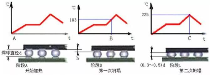
Figure 4 Chip Cold Solder Joints
图 5 Teared pad surface
3.Criterion of cold welding spot
IMC's incomplete growth and development, orange-peel surface and insufficient collapse height are the three most typical characteristics of μBGA and CSP cold-welded joints, which can usually be used as the criterion of μBGA and CSP cold-welded joints.
The IMC growth and development in reflow soldering is incomplete (it has been analyzed and introduced before, so it will not be repeated here)
Orange peel and collapse height less than μBGA on the surface, orange peel on the surface of CSP cold solder joint and collapse height less than μ BGA on the surface, which are unique physical phenomena of cold soldering. The formation mechanism can be described as follows:
During reflow soldering of μBGA and CSP, due to the joint action of the gravity and surface tension of the package, under normal circumstances, they all have to go through the following three basic stages: heating in stage A → first collapse in stage B → second collapse in stage C, as shown in Figure 6.
If the reflow soldering process only goes to the first collapse of stage B, and can't continue to go to stage C due to insufficient heat supply, a cold solder joint will be formed.
图 6 μBGA、CSP Physical and chemical process of reflow soldering
(1) stage a: when heating is started, the shapes of the solder joints of μBGA and CSP are shown in fig. 7.
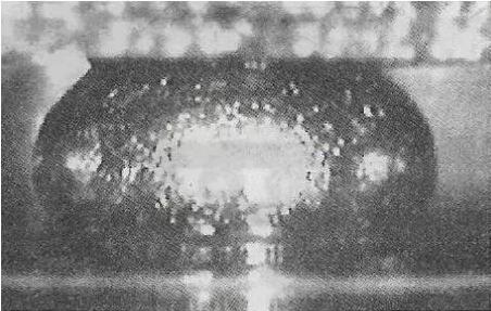
图 7 开始加热时的形态
(2) Stage B: After the first stage of heating, when the solder ball approaches and passes the melting point temperature, it will undergo a vertical collapse and its diameter will begin to increase. At this time, the solder is in a paste state where liquid and solid phases coexist. Because the heat is not purchased, the metallurgical reaction between solder balls and pads is weak, and the surface state of solder balls is rough and dull, as shown in Figure 8.
图 8 The morphology of solder ball when it approaches or passes its melting point.
(3) Stage C: When further heating, the solder ball reaches the peak temperature, and the metallurgical reaction between the solder ball and the bonding pad begins, resulting in the second collapse. At this time, the solder ball becomes flat, forming a horizontal truncated cone shape, and the surface presents a smooth and bright structure. The formation of interface layer greatly improves the mechanical strength and electrical properties of solder joints. At this time, the height of the chip off the board is reduced by 1/3 to 1/2 compared with the initial height, as shown in Figure 9.
图 9 Solder joints formed after normal reflow soldering.
From the physical and chemical processes of μBGA and CSP in reflow soldering described above, it can be seen that the formation of cold solder joints is almost always due to insufficient heat supply in the B stage of reflow soldering. The reflow soldering process is finished before the peak temperature is reached. Therefore, when the micro-optical vision system is used to inspect the quality of μBGA and CSP solder joints, the degree of cold welding can be judged according to the degree of orange peel on the surface of solder balls and the collapse height.
4.Analysis of defect degree of cold welding spot
Slight cold welding is a hidden defect, which will not seriously affect the normal function of the product for a period of time in a good use environment. Because the growth of IMC is not only a function of temperature, but also related to time. Although IMC is not well developed during reflow soldering, it can continue to grow and develop in use, but the growth rate is very slow. In order to accurately locate and evaluate the degree of cold welding, ERSACOPE is temporarily divided into three grades: Class A (slight cold welding), Class B (moderate cold welding) and Class C (severe cold welding) according to the actual observation results of Ersacope, as shown in Figure 10.
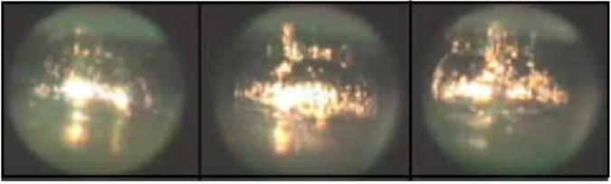
A 类(左)B 类(中)C 类(右)
图 10 Classification of cold welding
According to the actual observation results, it is found that A and B are the most common. Further metallographic analysis of three types of solder joints A, B and C is carried out, and the results are as follows.
1) class a. The mirror image of the slice analysis of Class A solder joint is shown in Figure 11. The IMC (alloy) on the interface is not obvious and has the characteristics of cold welding, but the interface is tightly bonded and no microcracks are found.
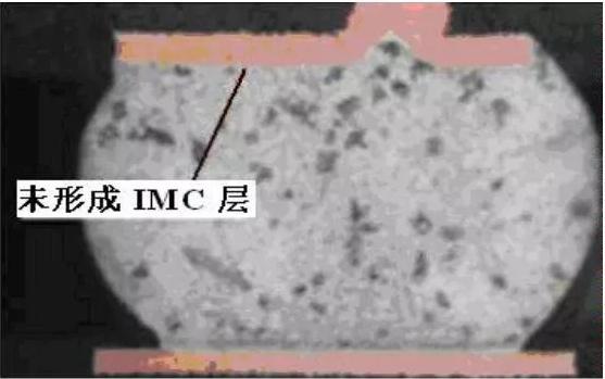
图 11 A 类焊点切片
2) Class B. The mirror image of the slice analysis of Class B solder joint is shown in Figure 12. The IMC of the interface is not obvious, the interface bonding is good, no microcracks are found, but the solder grains are not uniform.
3) Class C. The mirror image of C-type solder joint slice analysis is shown in Figure 13. No IMC (alloy) is formed on the interface, but penetrating cracks appear on the interface. The outer surface of the solder ball is irregular and uneven.
Conclusion: Category A and B can be accepted at discretion in situations with non-high reliability requirements, while category C should be rejected.
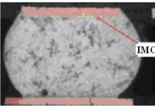
图 12 B Solder-like slice

图 13 C 类焊点切片
5.Causes and countermeasures of induced cold welding
1)Reasons for high cold welding rate of μBGA and CSP in hot air reflow soldering
Hot air convection uses air as the medium to conduct heat, which is ideal for heating components that "protrude" from the PCB surface, such as high pins and small components. However, in this process, due to the influence of the "boundary layer" formed between convection air and PCB, the gap between μBGA, CSP and PCB surface is close to the thickness of boundary layer, and it is difficult for hot air to penetrate into the bottom gap, so the conduction efficiency will be obviously reduced when heat is conducted to the bottom pad areas of μBGA and CSP, as shown in Figure 14.
图 14 Boundary layer causes hot air to affect μBGA, CSP Poor heat transfer in the bottom pad area
Under the same peak temperature and reflow time, compared with other components with good solder joint exposure in hot air, the heat obtained by the solder joints of μBGA and CSP will be obviously insufficient, resulting in some solder joints at the bottom of μBGA and CSP not reaching the wetting temperature and causing cold welding, as shown in Figure 15.
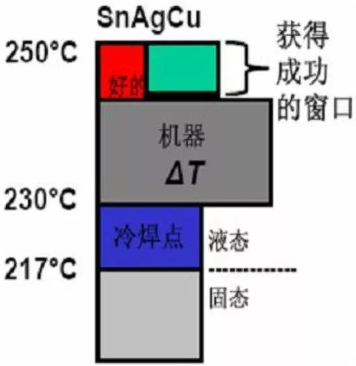
图 15 Cause of cold welding
Under the above state, in the reflow soldering process of μBGA and CSP, the heat transfer can only be that μBGA, CSP package and PCB are heated first, and then the package and PCB substrate are conducted to the solder pads and solder balls of μBGA and CSP to form solder joints.
For example, if the hot air of 240℃ acts on the surface of the package, the solder pads, μBGA and CSP solder balls will gradually heat up, and the temperature rise will have a lag time compared with other components. If it cannot rise to the required wetting temperature within the required reflow time, cold welding will occur.
2)Possible measures to solve the high incidence of cold welding in μBGA and CSP
(1) Adopt trapezoidal temperature curve (extending the peak temperature time)Reducing the peak temperature of reflow properly and prolonging the peak temperature time can improve the temperature difference between heat dissipation capacity components and large heat capacity components, and avoid overheating of smaller components.A modern compound reflow soldering system can reduce the temperature difference between 45mm BGA and SOP to 8℃.
(2) Improve the heat supply mode of reflow soldering.Reflow soldering is to solder thousands of components on the PCB substrate. If there are components with different mass, heat capacity and area on a PCB at the same time, the temperature will be uneven. At present, the two most common ways of re-flow heat supply in the industry and their characteristics are as follows.
① Forced convection heating. Forced hot air convection reflow soldering is a reflow soldering method that uses convection jet nozzle to force air flow to circulate, so as to heat the welded parts, as shown in Figure 16. The temperature of PCB substrate and components using this heating method is close to the gas temperature in a given heating area, which overcomes the problem of large temperature difference between components caused by infrared heating due to factors such as appearance color difference and surface reflection of components.
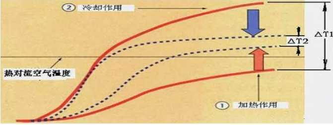
图 16 Forced hot air convection heating
As far as heat exchange is concerned, the heat transmission of this heating mode is worse than that of infrared, so the production efficiency is not as high as that of infrared heating mode, and the power consumption is more. In addition, due to the small heat transfer, the difference of heating rate among components will become larger due to the influence of the size of components.
The convection velocity of circulating gas is very important in forced hot air convection reflow welding equipment. In order to ensure that the circulating gas can act on any area of PCB, the gas flow must have sufficient speed or pressure. To some extent, it is easy to cause problems such as the jitter of thin PCB substrate and the displacement of components.
② Infrared heating. Infrared ray (IR) is an electromagnetic wave with a wavelength of 3 ~ 10 μ m. Usually, PCB, soldering flux, packaging of components and other materials are composed of molecular layers with atomic chemistry. These high-molecular substances are constantly vibrating due to molecular expansion and contraction and angle change. When the vibration frequency of these molecules comes into contact with similar infrared electromagnetic waves, these molecules will resonate and the vibration will become more intense. Frequent vibration will cause heat, heat
It can be quickly and equally transmitted to the whole object in a short time. Therefore, the object does not need to be heated at a high temperature from the outside, and it will be fully heated.
The advantages of infrared reflow soldering are: the surface of the same object is uniformly heated according to the irradiation, the thermal stress generated by the welded piece is small, and the thermal efficiency is high, thus saving energy.
The advantages of infrared reflow soldering are: the surface of the same object is uniformly heated according to the irradiation, the thermal stress generated by the welded piece is small, and the thermal efficiency is high, thus saving energy.
而它的缺点是:按同时照射的各物体,因其表面色泽的反光程度及材质不同,彼此间吸收的热量的不同而导致彼此间出现温差,个别物体因过量吸收热能而可能出现过热。
③ "IR+forced convection" isMain technical means to solve the cold welding of μBGA and CSP. For the welding between QFP140P and PCB and between 45mm BGA and PCB, it is found in foreign countries that when there is only convection heating or "IR+ forced convection" composite heating system, the difference of temperature uniformity under the two conditions is as follows:
a)Heat convection → the temperature difference between →QFP140P and PCB is 22℃;
b)“IR+强制对流”加热→QFP140P 与 PCB 之间的温差只有 7℃,而对 45mm的 BGA 温差进一步减小到 3℃。
The basic concept of "IR+ forced convection" heating is: using infrared rays as the main heating source to achieve the best heat conduction, and grasping the balanced heating characteristics of convection to reduce the temperature difference between components and PCB. Convection heating is helpful for heating components with large capacity, and notification is also helpful for cooling components with small heat capacity when they overheat.
图 17 Combined heating effect of "IR+ forced convection"
In Figure 17:
① represents the heating curve of components with large thermal capacity;
② is the heating curve of components with small heat capacity.
If only one heat source, whether IR or convection, is used, the heating effect shown by the thick solid line in fig. 17 will occur. The heating curve described by the dotted line in Figure 2 shows the advantages of "IR+ forced convection" combined heating (△T <△T). Here, the effect of increasing forced convection is: heating components below the temperature of hot air; At the same time, the components that have risen above the temperature of hot air are cooled.
At present, the most advanced reflow furnace technology combines the advantages of infrared radiation heating in river basin. The maximum temperature difference between components can be kept within 8℃, while the temperature difference between PCBs can be stabilized at about 1℃ during continuous mass production.
3)Influence of different installation positions on the incidence of cold welding
The phenomenon of cold welding of μBGA and CSP is also closely related to its mounting position on PCB.
Fig. 18 shows that two CSP chips (IC/A and IC/B) are jointly installed in a shield. The overall size and thickness of the chip IC/A are smaller and thinner than those of the chip IC/B, and there is a large space between it and the shield frame. From the effect of hot air reflow soldering, IC/A should be better than chip IC/B.
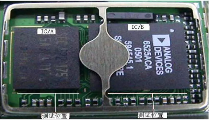
图 18 Influence of installation position on the incidence of cold welding
After reflow soldering the PCBA components shown in Figure 18 in the 7-temperature zone ("IR+ hot air") compound furnace and the 10-temperature zone pure hot-blast furnace, the ERSA SCOPE-30000 micro-optical vision monitoring system was used along the test position shown in the figure to directly capture the appearance image of the solder joint concerned. The results are shown in Table 1.
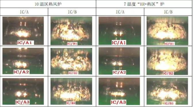
表 1 Influence of chip mounting position and heating mode on cold welding
From the micro-optical images shown in Table 1, the following conclusions can be clearly drawn:
(1) Whether it's a pure hot-blast stove with 10 temperature zones or a compound stove with 7 temperature zones ("IR+ hot air"), from the reflow soldering effect, the cold soldering rate of chip-to-IC/B is much higher than that of chip-to-IC/A. It shows that the installation position has great influence on the cold welding rate of μBGA and CSP.
(2) According to the classification and comparison of the photos, the reflow soldering effect of the ("IR+ hot air") compound furnace with 7 temperature zones is better than that of the pure hot-blast stove with 10 temperature zones, both in IC/A position and IC/B position. It shows that "IR+ hot air compoundHeating method is really effective in suppressing the cold welding of μBGA and CSP in reflow soldering.
三.虚焊和冷焊的异同
1.similarity
There are many similarities between virtual welding and cold welding in terms of phenomena, which is the reason why they are often mistaken in practice. Therefore, it is very important to accurately identify the similarities and differences between virtual welding and cold welding for quality control in electronic product manufacturing.
The similarity between virtual welding and cold welding is mainly manifested in the following aspects:
1) The solder joint failure caused by cold welding and virtual welding is characterized by interface failure, that is, the poor electrical contact or micro-crack of the solder joint occurs at the interface where the solder pad and solder are in contact;
2) The definitions of cold welding and virtual welding are similar, and the required intermetallic compound layer (interface alloy layer or IMC for short) is not formed at the interface, as shown in Figure 19 and Figure 20;
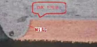
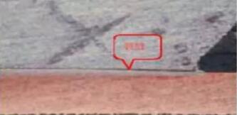
图 19 IMC 不明显
图 20 界面出现微裂缝
3) The effects and harms in engineering applications are similar, that is, there are poor electrical contact, unstable electrical performance and poor connection strength. Especially for μBGA and CSP, this solder joint defect is hidden,It takes a few days, months or even last year to be exposed.
2.Differences and physical positioning
1) The formation mechanism is different:
Virtual welding is caused by oxidation, vulcanization or pollution of the surface of the metal to be welded, which makes it impossible to weld, while cold welding is caused by insufficient heat supplied during welding.
2) The solutions are different:
Generally, virtual soldering can be completely solved by improving the cleanliness and weldability of the metal surface to be soldered and adjusting the chemical activity of flux, which is relatively easy to realize. While cold welding must solve the problem of sufficient heat in the welding process.
The supply problem, especially for high-density devices such as μBGA and CSP, often involves the heating mode of reflow oven and the efficiency of heat conversion and transfer. Therefore, it is difficult to cover a wide range.
3) Connection strength is different:
During virtual welding, because there is an oxide film between the solder and the base metal surface, the adhesion of the solidified solder is very poor and the connection effect is weak. The IMC layer formed on the solder joint interface with slight cold welding is very thin and incompletely developed, while the solder joint interface with serious cold welding is often accompanied by penetrating cracks and has no strength at all, as shown in Figure 21.
图21 界面出现贯穿性裂缝
4) The metallographic structure is different.
The metallographic structure after virtual welding slice is fine, as shown in Figure 22; However, the microstructure after cold welding is uneven, as shown in Figure 23.

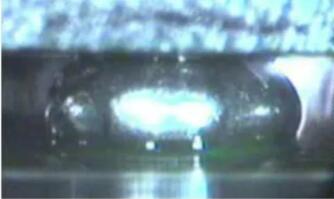
图 22 虚焊
图 23 冷焊
5) Different micro-optical visual images
(1) Good visual image of solder joints.
① During ①CBGA→CBGA reflow soldering, because the solder balls do not melt, the solder paste is fully filled and wetted between the solder pads and solder balls after reflow, with a good wetting angle, smooth surface and no collapse in height, as shown in Figure 24.
② The surface of PBGA → ball solder joint is bright and smooth, with good wetting angle, and the collapse height is about (1/3 ~ 1/2) of the height of ball pin. As shown in Figure 25.
图 24 CBGA
图 25 PBGA
(2)Visual image of virtual solder joints
The micro-optical visual image of the virtual solder joint is characterized in that the solder joint does not form wetting fillet, as shown in Figure 26;
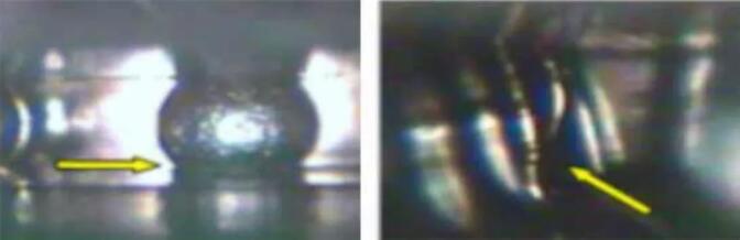
图 26 虚焊
(3)Visual image of cold welding spot;
The micro-optical visual images of cold solder joints are characterized by:
①The surface of the solder joint is orange peel, as shown in Figure 27.
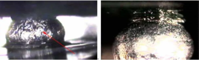
图 27 冷焊
②The reflow of solder paste is insufficient, as shown in Figure 28.
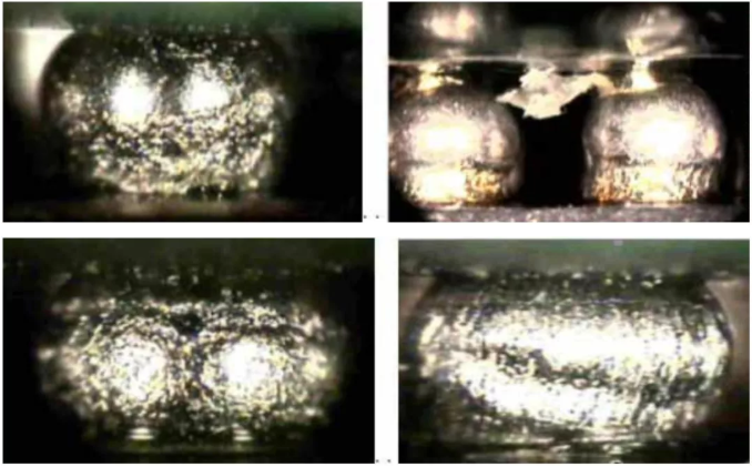
图 28 再流不充分
③Insufficient collapse height: only the first-stage collapse occurred, but it did not enter the second-stage collapse due to insufficient heat, as shown in Figure 29.
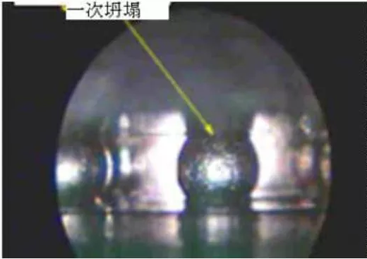
图 29
四.若干电子装联焊接缺陷的定义
1.Citation standards and documents
Insufficient collapse height
1)QJ aerospace standard
There is no uniform definition of some electronic assembly welding defects at home and abroad, which brings many twists and turns.
Zhang Yongzhong, from the Second Academy of Aerospace Sciences, said, "My view on virtual welding is to look at intermetallic compounds. In 2013, the Science and Technology Group also made a special topic of virtual welding, which was distributed to all units by the Quality Department of the Group in the form of quality briefing. The definition of virtual welding in it quoted the definition of virtual welding in QJ standard, but it was extended. It can be divided into explicit virtual welding (also called generalized virtual welding), implicit virtual welding, and explicit virtual welding means that the appearance can be checked. "
The QJ standard mentioned by Zhang Yongzhong of the Second Academy of Aerospace Sciences is QJ2828 "Electronic Assembly Terminology", which the author will refer to many times in the future. It was put forward by Aerospace 708, and China's aerospace standard formulated with reference to NASA standard of NASA and American MILL is still valid.
2) American IPC standard
The author also quoted the American IPC standard here. It should be noted that the IPC standard is a commercial standard formulated by "IPC American Connected Electronics Association".
IPC-A-610E CN "Acceptability of Electronic Components" published in April, 2010, in the section 5.2 Welding Abnormality, summarized the welding defects as: exposed metal substrate, pinhole/blowhole, incomplete reflow of solder paste, non-wetting,There are 14 categories of solder/rosin solder connection, dewetting, solder ball/splash, bridging, solder mesh/splash, solder disturbance, solder crack or crack, solder tip, lead-free filling warping and lead-free hot tearing/hole shrinkage, which are incomplete.
3) Works of Professor Fan Rongrong
The author also quotes Professor Fan Rongrong's definition of some welding defects below. Professor Fan Rongrong is a leading figure in China's electronic assembly industry, a winner of seven United Nations patents, and an outstanding young and middle-aged scientist in China in 1980s.
2.Misunderstanding of the definition of welding defects
Actually, virtual welding is only for open in Ipc, but IPC-A-610E doesn't say virtual welding or open. Open means open circuit. The term "open circuit" exists in China, but it is not found in the welding defects of IPC-A-610E.
Non-wetting, false welding, empty welding, open circuit and virtual welding, some of which belong to "common sayings" rather than terms, have different definitions.
The fundamental feature of virtual welding is that intermetallic compounds do not meet the requirements.The open circuit is not necessarily caused by virtual welding.
For example, "erecting a monument" is also an open circuit, but it is not virtual welding;Non-wetting and virtual welding have different meanings, but non-wetting will definitely lead to virtual welding;Virtual welding is not a derivative of China, but an objective fact.
3.rosin joint
1) When the welding parameters (temperature, time) are all normal, any phenomenon that intermetallic compound (IMC) with appropriate thickness is not formed on the connection interface during the welding process can be defined as virtual welding. —— Fan Rongrong, 1100 Questions on the Application of Modern Electronic Assembly Engineering, 2011.
2) The definition of virtual soldering in 2)QJ2828 is: the virtual soldering Pseudo soldering solder is isolated from the metal surface of the weldment by oxidation or other dirt, and no metal alloy layer is formed, but the defect is simply attached to the surface of the weldment.
4.cold welding
1) the minimum required wetting temperature is not reached between the solder and the base metal during welding; Or the phenomenon caused by incomplete metallurgical reaction, although local wetting occurs, can be defined as cold welding. —— Fan Rongrong, 1100 Questions on the Application of Modern Electronic Assembly Engineering, 2011.
2)QJ2828 defines cold welding as: if the welding temperature of cold solder joint is too low, the solder may solidify before wetting and flowing, and the appearance of solder joints cannot be smooth and bright, which is a defect that the welding quality is worse than that of virtual welding.
3)IPC-610D defines the cold solder joint as: cold solder joint-refers to the solder joint with poor wettability, gloomy appearance and looseness. (This phenomenon is caused by excessive impurities in solder, insufficient cleaning before welding, and/or insufficient heat during welding)
4)IPC-T-50 defines the cold welding connection as: the welding connection shows poor wetting and gray porous appearance. (This is due to excessive solder impurities, insufficient cleaning before welding, and/or insufficient heat during welding. )
图 30
焊接连接呈现不良的润湿,可能有截留的松香迹象,导致待连接的表面分离。
5.moisten
QJ2828 defines wetting as the phenomenon that wetting molten solder adheres to the surface of the welded metal to form a fairly uniform, smooth and continuous solder film.
6.Semi-wetting
QJ2828 defines semi-wetting as: after semi-wetting dewetting molten solder adheres to the surface of the welded metal, it retracts and leaves irregularities.The solder bumps, but the phenomenon that the base metal is not exposed.
7.Dewetting
IPC-T-50 defines dewetting: a condition in which molten solder is coated on the metal surface and then the solder retracts, resulting in the formation of an irregular solder pile with separated areas covered by a thin film and not exposed to the metal substrate or surface coating.
图 31
退润湿现象导致焊接连接不满足表面贴装或通孔插装的焊料填充要求。
8.nonwetting
1)QJ2828 defines non-wetting as the phenomenon that the non-wetting molten solder contacts with the metal surface, and only part of it adheres to the surface and still exposes the base metal.
2)IPC-T-50 definition of non-wetting: molten solder can't form metal bond with metal base material (base material).
a)元器件端子不润湿
b)导线端子不润丝
五.结语
After nearly 40 years of rapid development of SMT in China, people in the industry are increasingly aware of the importance of quality and reliability, and SMT assembly and welding technology and testing technology are developing rapidly. However, the lag of standards, including the lag of various definitions and terms, has affected the development of SMT industry. China's existing terminology standards related to electronic assembly standards were basically introduced in the mid-1990s. However, there are some problems in terms and definitions in IPC standards, which do not fully adapt to China's national conditions.
Therefore, it is normal for some different understandings of terms and definitions to appear. China's expected standards can meet the needs of manufacturing development. For reference only. (Author of this article: Chen Zhenghao, 10 Institute of China Electric Power)
Disclaimer: This article is reproduced from "actSMTC". This article only represents the author's personal views, and does not represent the views of Sacco Micro and the industry. It is only for reprinting and sharing to support the protection of intellectual property rights. Please indicate the original source and author when reprinting. If there is any infringement, please contact us to delete it.


Site Map | 萨科微 | 金航标 | Slkor | Kinghelm
RU | FR | DE | IT | ES | PT | JA | KO | AR | TR | TH | MS | VI | MG | FA | ZH-TW | HR | BG | SD| GD | SN | SM | PS | LB | KY | KU | HAW | CO | AM | UZ | TG | SU | ST | ML | KK | NY | ZU | YO | TE | TA | SO| PA| NE | MN | MI | LA | LO | KM | KN
| JW | IG | HMN | HA | EO | CEB | BS | BN | UR | HT | KA | EU | AZ | HY | YI |MK | IS | BE | CY | GA | SW | SV | AF | FA | TR | TH | MT | HU | GL | ET | NL | DA | CS | FI | EL | HI | NO | PL | RO | CA | TL | IW | LV | ID | LT | SR | SQ | SL | UK
Copyright ©2015-2025 Shenzhen Slkor Micro Semicon Co., Ltd
