Service hotline
+86 0755-83044319
release time:2024-01-31Author source:SlkorBrowse:19619
(Following part I: Integrated circuit design; Part II: Integrated Circuit Manufacturing)
V. ATP (Assembly, Test, andPackaging) and advanced packaging
Basic conclusions about assembly, testing, packaging and advanced packaging:
(1) For the relatively low-tech back-end semiconductor ATP, the United States relies heavily on foreign resources concentrated in Asia.
(2) As chips become more complex, advanced packaging methods represent potential areas for significant technological progress. However, the US is also not a cost-effective place to develop a strong advanced packaging industry because it lacks the necessary materials ecosystem;
(3) In response, heavy Chinese investment could disrupt existing markets.
(I) Flag State's basic estimates of basic packaging and testing
(A) Basic information
At the back-end basic ATP stage, the chip (core) is assembled into a finished product, which is tested, packaged, and assembled into electronics. There are two modes for the ATP stage :(1) OEM by IDM and (2) OEM. Foundries are OSAT (pure semiconductor Assembly and Testing) companies that specialize in testing, packaging, assembly or assembly and provide contract services. In terms of the total ATP market, US companies accounted for 28% of the total revenue; Although US companies account for approximately 43% of the vertically integrated IDM ATP revenues, US companies have outsourced ATP production to facilities outside the US. Foundries such as [敏感词] ([敏感词]), UMC ([敏感词]), SMIC (Mainland China) and XMC (Mainland China) have entered the packaging business to increase the manufacturing services they offer to fabless customers, especially for advanced packaging of small chips. [敏感词] launched its first advanced packaging solution in 2012. In 2017, there were more than 100 different OSATS on the market. There are eight large OSATS; Most are small to medium sized players.
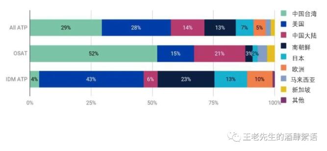
Although there are some US OSAT companies (notably Amkor), US companies account for only 15% of OSAT's business ([敏感词] leads with 52%, followed by China with 21%), and Amkor is based in the US but does not have a manufacturing facility in the US.
Basic ATP has traditionally been a highly automated and low-value business, requiring considerable footprint and employing mostly low-skilled workers (this is changing with the introduction of the advanced packaging technologies discussed below). Thus, this operation was the first phase (beginning in the 1970s) of the outsourcing of production in the United States, which was mainly to southeast Asia. Today, most ATP outsourcing plants are in China, [敏感词] and Southeast Asia (Singapore, Malaysia, Philippines and Vietnam). SEMI and Techsearch identified more than 120 OSAT outsourcing companies and 360 packaging plants worldwide in 2018. Of the 360 factories, there are more than 100 in China, about 100 in [敏感词] and 43 in Southeast Asia (the others are in Europe or The Americas). OSAT production in China uses the current mainstream packaging technology, but China is developing advanced packaging technology.
On the testing side, semiconductor technologies must be certified and tested before they can be used in temperature ranges (extended range), radiation resistance and harsh environments for national security reasons. This includes single-particle effects (SEE) testing using the heavy ion radiation testing infrastructure. The existing heavy ion radiation testing infrastructure in the United States is fragile and cannot meet current or future SEE testing needs. Customers often experience long waiting times and rising test prices, and are vulnerable to significant stress even if a major facility suddenly shuts down. "There are fewer than half a dozen accelerator LABS that can produce ion beams of sufficient ion variety and energy to meet SEE testing requirements." This affects the availability of tests to support future space missions between space agencies and industry (including satellites).
(B) Major risks
Today, the United States has only 3 percent of global semiconductor packaging capacity (excluding testing capacity), mainly provided by IDM companies, which often have ATP facilities outside the United States. While this has historically been a low-tech component of the supply chain, it is a critical step. America's reliance on essential ATP production in Southeast Asia, [敏感词] and China exposes the US supply chain to disruption.
(II) Citibank's discussion on advanced packaging technology
(A) Basic information
While basic ATP has traditionally been a low-value component of the supply chain, packaging technologies are becoming increasingly advanced. For decades, the semiconductor industry has kept pace with Moore's Law, which predicts that the number of transistors on a semiconductor doubles roughly every two years. Today, the power and performance benefits of shrinking chip sizes at each new process node are decreasing, while the cost per transistor is increasing. While downsizing is still an option, as scaling becomes more expensive and difficult, the semiconductor industry is looking for alternatives that involve assembling small chips and/or multiple integrated circuits into a single package. This is called advanced encapsulation. Advanced packaging represents an alternative and complementary technology to line-width reduction because it provides higher chip density at the package stage rather than the chip level and allows for the integration of different chip functions within a single package. Advanced packaging also allows for greater use of commercial-off-the-shelf ([敏感词]-approved) chips to customize solutions.
Advanced packaging types include chip stacking techniques (especially memory chips) and embedded chips, fan-out, wafer-level packaging, and system-level packaging (assembling small chips or multiple chips into a single package). One approach to logic chips is to separate standardized IP functions into different, smaller chips, called "microchips," connected through standard interfaces on a single package. Small chips work with other small chips, so designs must be optimized together and cannot be designed in isolation. The [敏感词] Advanced Research Projects Agency (DARPA) and the Navy, as well as industry players (AMD, Marvell, and Intel), have a number of projects exploring this approach. Advanced packaging is of national security value by breaking down function, safety, volume, and environmental performance to provide customizable equipment for unique national security applications.
Advanced packaging accounted for 42.6% of the total value of semiconductor packaging in 2019 and is expected to reach 2025. Will account for nearly half of the entire semiconductor packaging market. This would represent a compound annual growth rate (CAGR) of 6.1% between 2014 and 2025, with more advanced packaging revenues doubling from $20 billion in 2014 to approximately $42 billion in 2025. This is almost three times the expected growth of the traditional packaging market, with a projected CAGR of 2.2 per cent between 2014 and 2025.
The world's top 10 advanced packaging companies include: two IDM companies (Intel of the United States and Samsung Korea); [敏感词] is also one of the world's top 10 advanced packaging companies. The top five OSAT advanced packaging companies in the world include ASE ([敏感词]), SPIL ([敏感词]), Amkor (USA), Powertech Technology ([敏感词]) and JCET (China). In addition, there are two smaller OSAT companies, Nepes Display (Korea) and Chipbond ([敏感词]). The 10 companies process about three-quarters of advanced packaged chips.
Advanced packaging in the United States is primarily provided by IDM vendors, including Intel, Texas Instruments, and Micron. GlobalFoundries is a U.S.-based foundry that also provides advanced packaging services. In addition, smaller companies, such as Micross, Skywater and Qorvo, offer advanced packaging services to meet niche [敏感词] and industrial needs.
As mentioned above, while China does not currently have strong advanced packaging capabilities, it is developing advanced packaging capabilities to compensate for its lack of cutting-edge semiconductor production
As the capacity and demand for advanced packaging grows, comments submitted in response to a Federal Registration Notice of Investigation (NOI) pointed to the lack of advanced packaging substrates (based on printed circuit board technology) and vulnerabilities in the associated supply chain in the United States. Base material supplier is located in Asia. Major substrate companies include: Ibiden (Japan), Nanya ([敏感词]), Shinko (Japan), Samsung (Korea), Unimicron ([敏感词]), Shennan Circuits (China), Zhuhai Yueya (China) and AKM Electronics Industrial (China).
In addition, PCB manufacturing has moved to China, making it a more attractive market for substrate suppliers. IPC/ US Reliable Electronics Partnership (USPAE) estimates that the US is 20 years behind Asia in printing circuit board manufacturing technology for next-generation electronics applications, The U.S. once accounted for more than 30% of the world's printed circuit board manufacturing; now it accounts for less than 5%
(B) Major risks
China's investment in advanced packaging threatens future markets:
While China lacks a strong advanced packaging capability, the Chinese government has invested heavily in advanced packaging. Advanced packaging has been the technology focus of China's semiconductor industry for the past few years, with The State Council aiming for advanced packaging to account for about 30 per cent of all packaging revenues for Chinese suppliers by 2015. In January 2021, SMIC's newly hired vice chairman said That Chinese companies should focus on advanced packaging to overcome their weakness in reducing semiconductor line width, which could signal that SMIC will move aggressively into advanced packaging. Stephen Hiebert, senior Director of marketing at SEMICONDUCTOR Packaging KLA, reported in 2018 that "... We are seeing strong OSAT investments in China as advanced packaging capacity increases to match China's front-end fabs projects."
Insufficient capacity of advanced packaging materials:
Advanced packaging substrates are based on printed circuit board technology, which is mostly manufactured in Asia and mostly in China. This poses a challenge for companies seeking to invest in advanced packaging in the United States.
[敏感词] needs alone are not enough to keep advanced packaging technology in the US:
A small number of U.S. companies provide advanced packaging solutions for [敏感词] needs, and these companies have only a small market share. As advanced packaging capabilities grow outside the US, they will soon outnumber [敏感词] needs and market forces will attract cutting-edge capabilities overseas. Ultimately, quantity drives innovation and operational learning; Without commercial volume, the US will not be able to keep up with technology in terms of quality, cost or labor.
(3) Summary
In summary, the US relies on foreign resources concentrated in Asia for back-end ATP capacity, which creates supply chain disruption risk in this part of the supply chain. Encapsulation is becoming more advanced as the industry looks for new ways to compensate for the complexity of smaller and smaller feature sizes at the most advanced or smallest nodes, lower yields, and diminishing marginal returns. While the United States and its partners have advanced packaging capabilities, China's heavy investment in advanced packaging has the potential to disrupt the market in the future. In addition, the U.S. lacks an ecosystem to develop advanced packaging technologies.
Disclaimer: This article is reprinted from "Mr. Wang's Restaurant talk", this article only represents the author's personal views, does not represent the views of Sakwei and the industry, only to reprint and share, support the protection of intellectual property rights, reprint please indicate the original source and author, if there is infringement, please contact us to delete.


Site Map | 萨科微 | 金航标 | Slkor | Kinghelm
RU | FR | DE | IT | ES | PT | JA | KO | AR | TR | TH | MS | VI | MG | FA | ZH-TW | HR | BG | SD| GD | SN | SM | PS | LB | KY | KU | HAW | CO | AM | UZ | TG | SU | ST | ML | KK | NY | ZU | YO | TE | TA | SO| PA| NE | MN | MI | LA | LO | KM | KN
| JW | IG | HMN | HA | EO | CEB | BS | BN | UR | HT | KA | EU | AZ | HY | YI |MK | IS | BE | CY | GA | SW | SV | AF | FA | TR | TH | MT | HU | GL | ET | NL | DA | CS | FI | EL | HI | NO | PL | RO | CA | TL | IW | LV | ID | LT | SR | SQ | SL | UK
Copyright ©2015-2025 Shenzhen Slkor Micro Semicon Co., Ltd
