Service hotline
+86 0755-83044319

release time:2022-03-03Author source:SlkorBrowse:11903
With the progress and development of society, the application of MOS tube in the electronics industry is becoming more and more extensive. As a "silicon carbide expert" that can develop silicon carbide products, Sark Microex SLKOR must come to science in this regard.
MOS is the abbreviation of MOSFET, the full name is Metal Oxide Field Effect Transistor. It is a semiconductor device that uses the electric field effect of the input loop to control the current of the output loop. The structure, principle, characteristics, symbol rules and package types of MOS tubes are roughly as follows.
1. The structure of MOS tube:
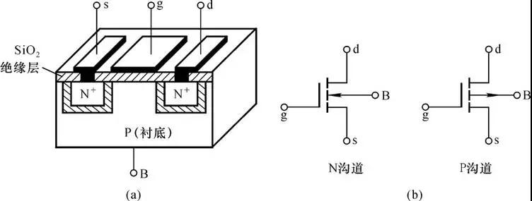
The structure of the MOS tube is to use semiconductor lithography and diffusion technology to make two N+ regions with high doping concentration on a P-type semiconductor silicon substrate with a low doping concentration, and use metal aluminum to lead out two electrodes, which are respectively used as drains. pole D and source S. Then, the surface of the P-type semiconductor between the drain and the source is covered with a thin silicon dioxide (SiO2) insulating film, and an aluminum electrode is installed on this insulating film as the gate G. This constitutes an N-channel (NPN type) enhancement MOS transistor. Its gate and other electrodes are insulated.
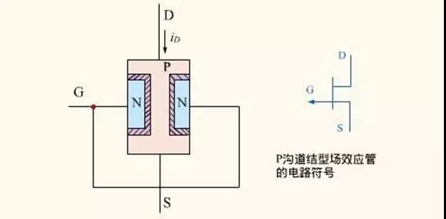
In the same way as above, on an N-type semiconductor silicon substrate with a low doping concentration, two P+ regions with high doping concentration are fabricated by semiconductor lithography and diffusion processes, and the same gate fabrication process as described above is used. Made into a P-channel (PNP type) enhancement MOS tube. (a) and (b) shown in Figure 1-1 are the structure diagram and representative symbol of the P-channel MOS pipeline, respectively.
2、MOS 管的工作原理:
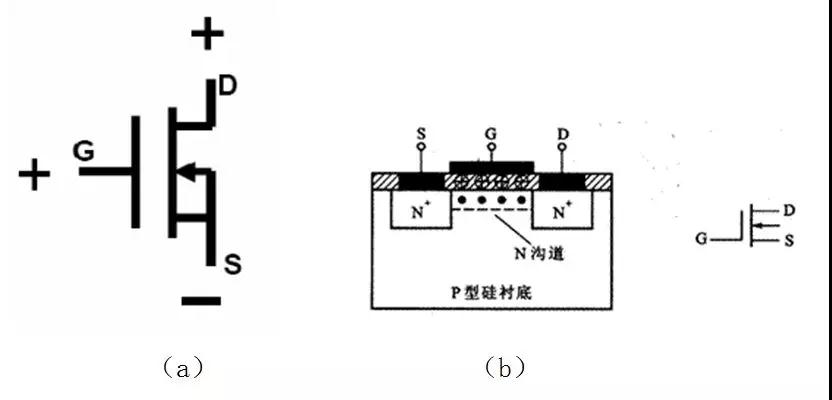
It can be seen from Figure 1-2-(a) that there are two back-to-back PN junctions between the drain D and the source S of the enhancement mode MOS transistor. When the gate-source voltage VGS=0, even if the drain-source voltage VDS is added, there is always a PN junction in the reverse bias state, and there is no conductive channel between the drain-source (no current flows), so at this time the drain Current ID=0. At this time, if a forward voltage is applied between the gate and the source, as shown in Figure 1-2-(b), that is, VGS>0, a gate will be generated in the SiO2 insulating layer between the gate and the silicon substrate. The electric field pointing to the P-type silicon substrate, because the oxide layer is insulating, the voltage VGS applied to the gate cannot form a current, and a capacitor is formed on both sides of the oxide layer. VGS is equivalent to charging this capacitor and forming a The electric field, as VGS gradually increases, is attracted by the positive gate voltage, and a large number of electrons are gathered on the other side of this capacitor and form an N-type conduction channel from drain to source. When VGS is greater than the tube's When the turn-on voltage VT (generally about 2V), the N-channel tube starts to conduct, forming the drain current ID. We call the gate-source voltage when the channel starts to form the turn-on voltage, which is generally represented by VT. Controlling the magnitude of the gate voltage VGS changes the strength of the electric field, so that the purpose of controlling the size of the drain current ID can be achieved.
3. Characteristics of MOS tube:
It can be seen from the working principle of the above MOS tube that the gate G and the source S of the MOS tube are insulated. Due to the existence of the SiO2 insulating layer, there is an equivalent capacitance between the gate G and the source S. , the voltage VGS generates an electric field which leads to the generation of source-drain current. The gate voltage VGS at this time determines the magnitude of the drain current, and the magnitude of the drain current ID can be controlled by controlling the magnitude of the gate voltage VGS. This leads to the following conclusions:
1) The MOS tube is a device that controls the current by changing the voltage, so it is a voltage device.
2) The input characteristic of the MOS pipeline is capacitive, so the input impedance is extremely high.
4. The voltage polarity and symbol rules of the MOS tube:
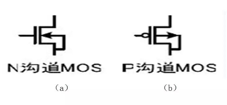
Figure 1-4-(a) is the symbol of N-channel MOS transistor. In the figure, D is the drain, S is the source, G is the gate, and the arrow in the middle represents the substrate. If the arrow is inward, it means that it is an N-channel The MOS tube, the arrow outward indicates that it is a P-channel MOS tube.
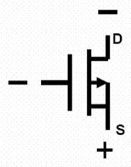
In fact, in the process of MOS tube production, the substrate is connected to the source before leaving the factory, so in the rules of the symbol, the arrow representing the substrate must also be connected to the source to distinguish the drain from the source. Figure 1-4-(c) is the symbol of P-channel MOS transistor. The polarity of the applied voltage of the MOS tube is the same as that of our ordinary transistor, the N-channel is similar to the NPN transistor, the drain D is connected to the positive electrode, the source S is connected to the negative electrode, and the conductive channel is established when the gate G is positive voltage, and the N-channel is connected. The MOS tube starts to work, as shown in Figure 1-4-(b). The same P-channel transistor is similar to the PNP transistor, the drain D is connected to the negative electrode, the source S is connected to the positive electrode, and the gate G is negatively charged, the conductive channel is established, and the P-channel MOS transistor starts to work, as shown in Figure 1-4-(d) shown.
N-channel MOS transistor symbol Figure 1-4-(a)
N-channel MOS transistor voltage polarity and substrate connection 1-4-(b)
(c)
(d)
P-channel MOS transistor symbol Figure 1-4-(c)
P-channel MOS transistor voltage polarity and substrate connection 1-4-(d)
5. The main package of MOS tube:
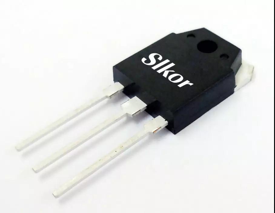
At present, the popular conventional packages include TO-220, TO-3P, TO-247 single-tube and various modules, and special packages can be provided according to the specific product requirements of customers. According to the common models and packages of Sako Micro SLKOR, we will sort them out as follows:
TO-3P
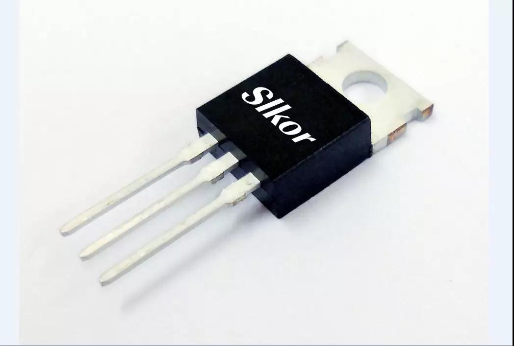
TO-220

TO-247
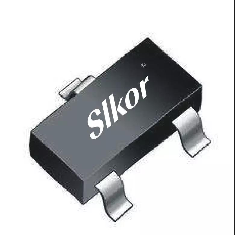
SOT-23
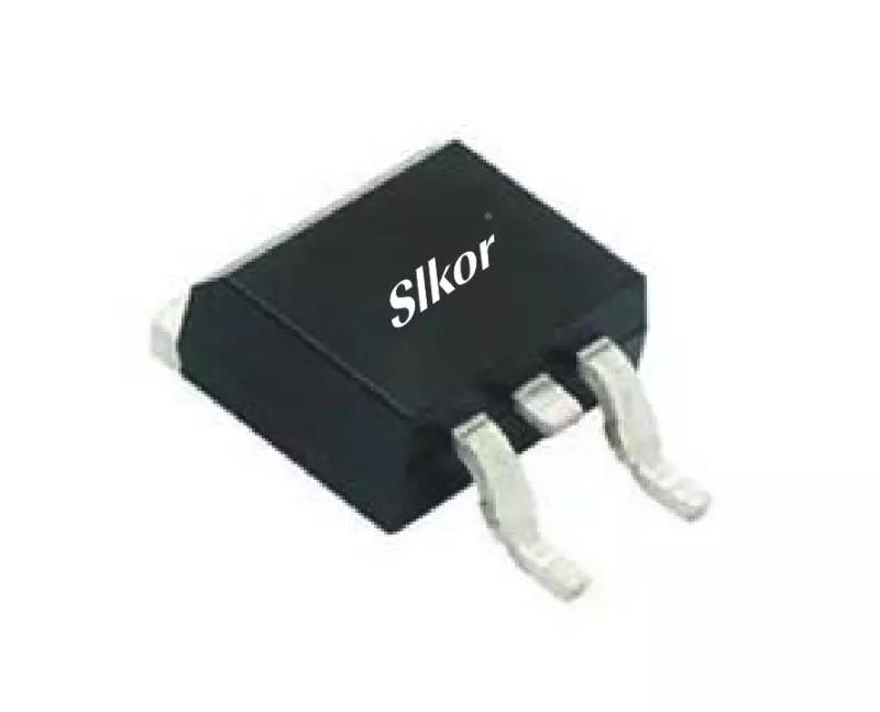
TO-252
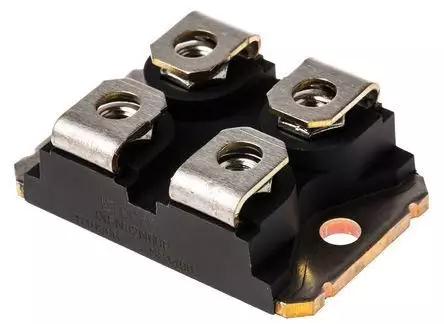
SOT-227B


Site Map | 萨科微 | 金航标 | Slkor | Kinghelm
RU | FR | DE | IT | ES | PT | JA | KO | AR | TR | TH | MS | VI | MG | FA | ZH-TW | HR | BG | SD| GD | SN | SM | PS | LB | KY | KU | HAW | CO | AM | UZ | TG | SU | ST | ML | KK | NY | ZU | YO | TE | TA | SO| PA| NE | MN | MI | LA | LO | KM | KN
| JW | IG | HMN | HA | EO | CEB | BS | BN | UR | HT | KA | EU | AZ | HY | YI |MK | IS | BE | CY | GA | SW | SV | AF | FA | TR | TH | MT | HU | GL | ET | NL | DA | CS | FI | EL | HI | NO | PL | RO | CA | TL | IW | LV | ID | LT | SR | SQ | SL | UK
Copyright ©2015-2025 Shenzhen Slkor Micro Semicon Co., Ltd
