Advanced packaging is a major technological highlight of the "More than Moore" era. As chip miniaturization becomes increasingly challenging and costly at each process node, engineers are opting to place multiple chips into advanced packaging instead of further shrinking individual chips. This article will provide a brief introduction to the ten most common terms in advanced packaging technology.
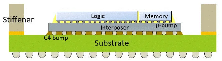
2.5D packaging
2.5D packaging is an advancement from traditional 2D IC packaging technology, allowing for more refined routing and spatial utilization. In 2.5D packaging, bare die stacks or side-by-side placements sit atop an interposer with silicon through-silicon vias (TSVs). The base, which is the interposer, facilitates connectivity between the chips.
2.5D packaging is commonly used in high-end ASICs, FPGAs, GPUs, and memory cubes. In 2008, Xilinx subdivided its large FPGA into four smaller, higher-yielding chips connected via a silicon interposer. This marked the inception of 2.5D packaging, later widely adopted for High Bandwidth Memory (HBM) processor integration.
2.5D Packaging Schematic Diagram
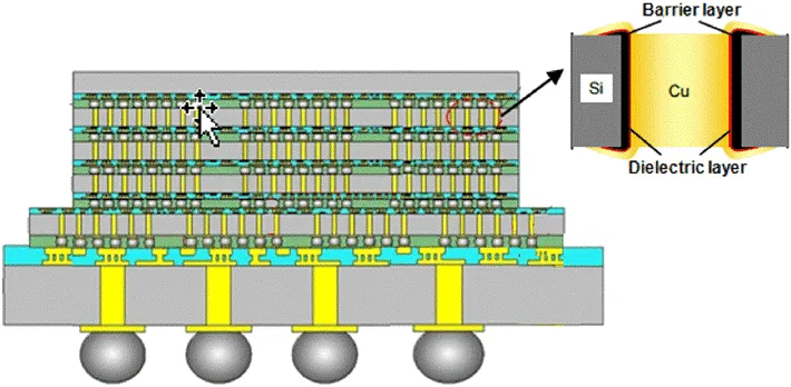
3D Packaging
In 3D IC packaging, logic die stacks together or with memory die stacks without the need for constructing a large System-on-Chip (SoC). The bare dies are interconnected through an active interposer layer. While 2.5D IC packaging utilizes conductive bumps or TSVs to stack components on the interposer, 3D IC packaging connects multiple layers of silicon wafers with TSV-enabled components.
TSV technology serves as a crucial enabling technology in 2.5D and 3D IC packaging, and the semiconductor industry has been using HBM technology to produce DRAM chips for 3D IC packaging.
From the cross-sectional view of 3D packaging, it can be observed that the vertical interconnection between silicon chips is achieved through metal copper TSVs.
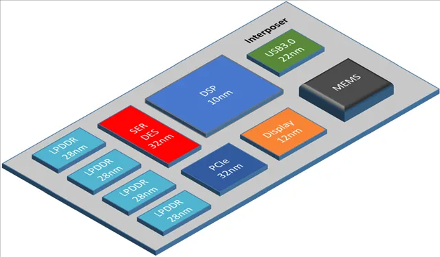
Chiplet
Within the chiplet library, there is a range of modular chips that can be integrated into packaging using die-to-die interconnect technology. Chiplets represent another form of 3D IC packaging, enabling the heterogeneous integration of CMOS and non-CMOS components. In other words, they are smaller System-on-Chips (SoCs), known as chiplets, rather than large SoCs within the package.
Breaking down large SoCs into smaller chips offers higher yields and lower costs compared to individual bare dies. Chiplets allow designers to leverage various IPs without being constrained by process nodes or manufacturing technologies. They can be fabricated using a variety of materials, including silicon, glass, and laminates.
A Chiplet-based system consists of multiple chiplets on an interposer layer
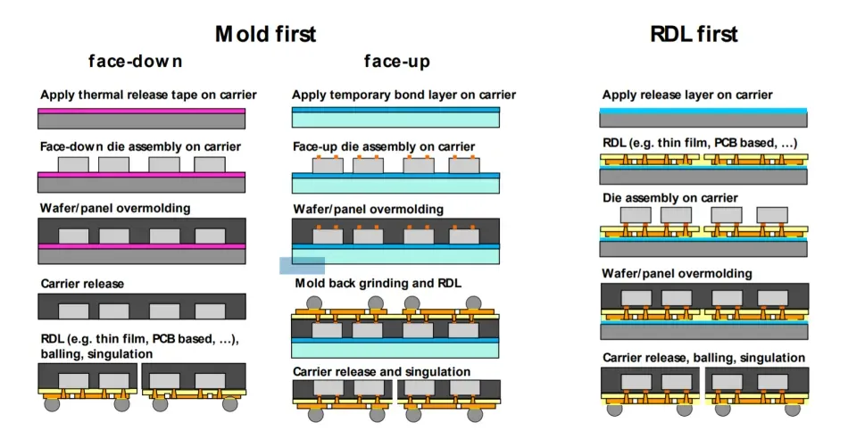
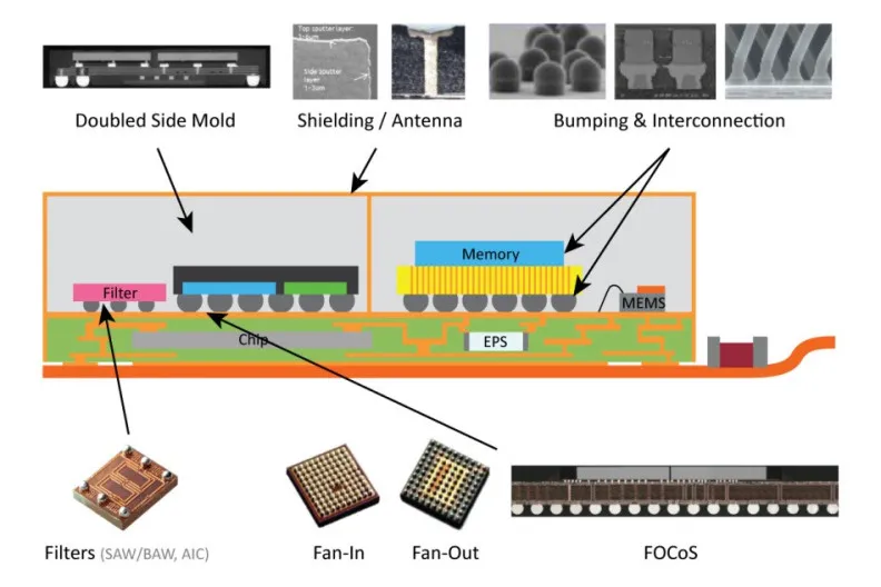
Fan-Out Packaging
In fan-out packaging, the "connections" are fanned out on the chip surface to provide more external I/O. It utilizes epoxy molding compound (EMC) to completely embed bare dies, eliminating process steps such as wafer bumping, underfill, flip-chip bonding, cleaning, bottom dispense, cure, and the need for an interposer layer, making heterogeneous integration simpler.
Compared to other packaging types, fan-out technology offers smaller form factors with more I/O. In 2016, it enabled Apple to integrate its 16-nanometer application processor with mobile DRAM using [敏感词]'s packaging technology into a single package for the iPhone 7, establishing itself as a technological standout.
Fan-Out Packaging
Fan-Out Wafer-Level Packaging (FOWLP)
FOWLP technology is an improvement upon wafer-level packaging (WLP) that enables more external connections for silicon chips. It involves embedding the chip in an epoxy molding compound, then constructing a high-density redistribution layer (RDL) on the wafer surface and applying solder balls to form a reconstituted wafer.
Typically, processed wafers are first diced into individual bare dies, which are then dispersed and placed on a carrier structure, with gaps filled to form the reconstituted wafer. FOWLP provides a significant number of connections between the packaging and the application circuit board, and because the substrate is larger than the bare die, the spacing of the bare dies is actually more relaxed.
Fan-Out Packaging
Heterogeneous Integration
Heterogeneous integration involves combining separately manufactured different components into a higher-level assembly, thereby enhancing functionality and improving operational characteristics. As a result, semiconductor component manufacturers can integrate functional components using different process flows into a single component.
Heterogeneous integration is similar to System-in-Package (SiP), but instead of integrating multiple bare dies on a single substrate, it involves integrating multiple IPs in the form of chiplets on a single substrate. The fundamental concept of heterogeneous integration is to combine multiple components with different functionalities into the same package.
Building Blocks of Heterogeneous Integration Technologies
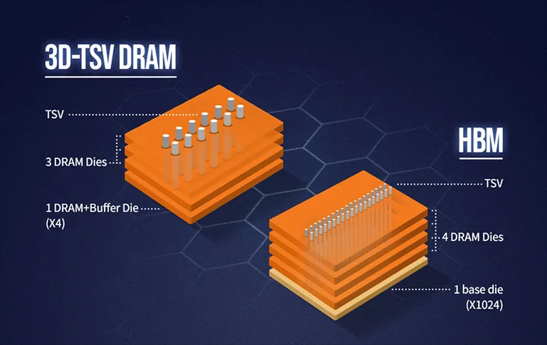
HBM
HBM is a standardized stacked memory technology that provides high-bandwidth channels for data within the stack and between memory and logic components. HBM packaging stacks memory dies together and connects them through TSVs to create more I/Os and bandwidth.
HBM, a JEDEC standard, vertically integrates multiple layers of DRAM components within the package alongside application processors, GPUs, and SoCs. HBM is primarily implemented in the form of 2.5D packaging for high-end servers and network chips. The latest version, HBM2, addresses capacity and clock speed limitations seen in the initial HBM version.
HBM
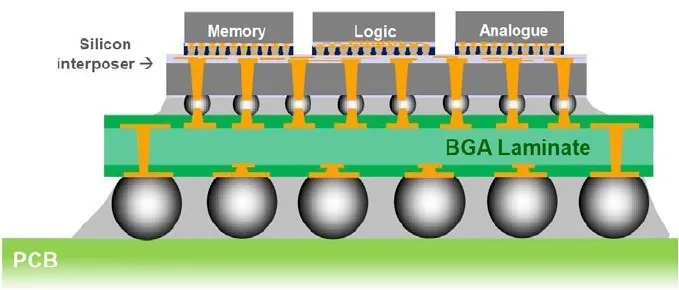
Interposer
An interposer is a conduit for transmitting electrical signals between multiple chip dies or circuit boards within a package. It serves as the electrical interface between sockets or connectors, enabling signals to travel longer distances and connect to other sockets on the board.
Interposers can be made of silicon or organic materials, acting as a bridge between multiple chip dies and circuit boards. Silicon interposers are a proven technology known for their high-density I/O and TSV formation capabilities, playing a crucial role in 2.5D and 3D IC chip packaging.
Typical Implementations of Interposer in System Partitioning
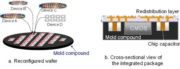
Redistribution Layer
The redistribution layer consists of copper interconnects or traces used to establish electrical connections between various parts of the package. It is a metal or high-polymer dielectric layer that allows bare dies to be stacked in the package, reducing the I/O pitch of large chip assemblies. The redistribution layer has become an integral part of 2.5D and 3D packaging solutions, enabling chips on it to communicate with each other through the interposer.
Integrated Packaging Using Redistribution Layer
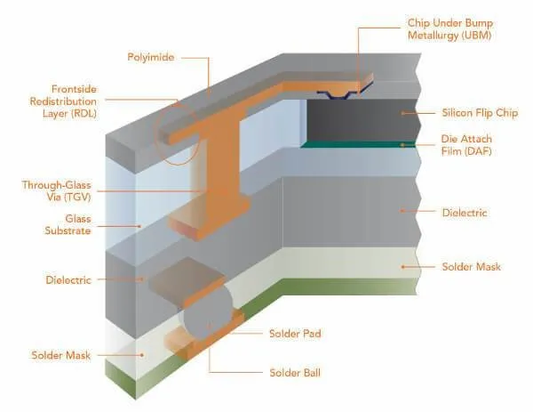
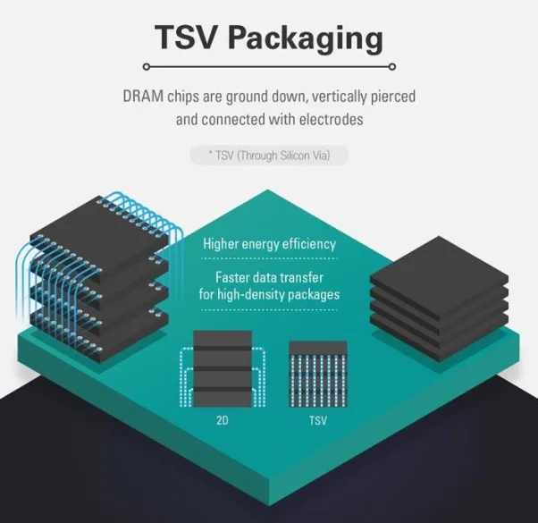
Through-Silicon Via (TSV)
TSV is a key enabling technology for 2.5D and 3D packaging solutions, involving the filling of copper in wafers to provide vertical interconnections through bare silicon wafers. It traverses the entire chip to facilitate electrical connections, creating the shortest path from one side of the chip to the other.
The process involves etching through-holes or cavities from the front side of the wafer to a certain depth, insulating them, and filling them with conductive material (typically copper). After chip fabrication, the wafer is thinned from the back side to expose the Through-Silicon Vias and the metal deposited on the backside of the wafer, completing the TSV interconnections.
In TSV packaging, DRAM chips are grounded, penetrated, and connected to electrodes