Service hotline
+86 0755-83044319
release time:2023-10-09Author source:SlkorBrowse:15231
In the current IGBT surface structure, planar and trench types can be said to be evenly matched. When many readers first encounter these two terms, they may mistakenly think that the current of the planar IGBT flows horizontally, while the current of the trench-gate IGBT flows vertically. In fact, this is a misunderstanding. Regardless of whether it is a planar or trench type IGBT, the current flows vertically. Moreover, for all power electronic devices that we are familiar with, such as IGBTs, MOSFETs, thyristors, and power diodes, in order to meet voltage withstand requirements, the current is made to flow vertically. For IGBTs, the hole current flows from the back collector electrode to the front emitter electrode; the electron current flows from the emitter, passes through the surface inversion channel, and flows to the back collector, as shown in Figure 1.
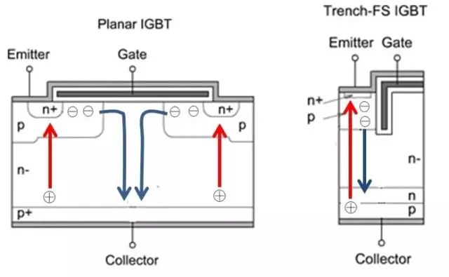
Figure 1. Current flow direction in IGBT
We all know that compared to planar IGBTs, trench-gate IGBTs can significantly reduce the on-state voltage drop without increasing the turn-off losses. So, how does the trench gate achieve this? It has three "tricks": elimination of the JFET effect, increased channel density, and increased near-surface carrier concentration.
Elimination of the JFET Effect
The main difference between the trench gate structure and the planar gate structure lies in the orientation of the inverted channel in the P-type emitter region when the IGBT is turned on. In the trench gate structure, the inverted channel is vertical instead of horizontal.
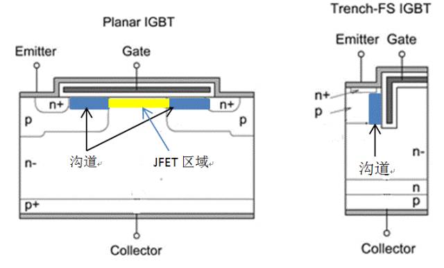
Figure 2. Schematic diagram of the inverted channel in planar and trench-gate IGBTs.
In planar gate IGBTs, during forward conduction, the PN junction formed between the P-well and the n-drift region is in a slight reverse bias state. This results in the formation of a space charge region with a certain width, which occupies a certain amount of space. As a result, the current can only flow through a relatively narrow space, increasing the impedance along the current path.
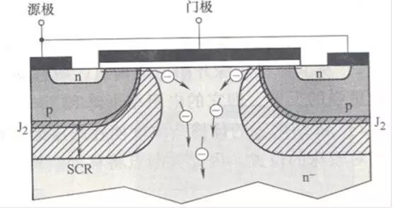
Figure 3. JFET effect in planar gate IGBT.
Therefore, in planar gate IGBTs, in the direction of electron flow, there is the channel resistance Rchannel, JFET resistance RJFET, and the drift region resistance Rn-. On the other hand, in trench-gate IGBTs, the vertical trench structure eliminates the JFET region, resulting in a lower overall impedance along the current path.
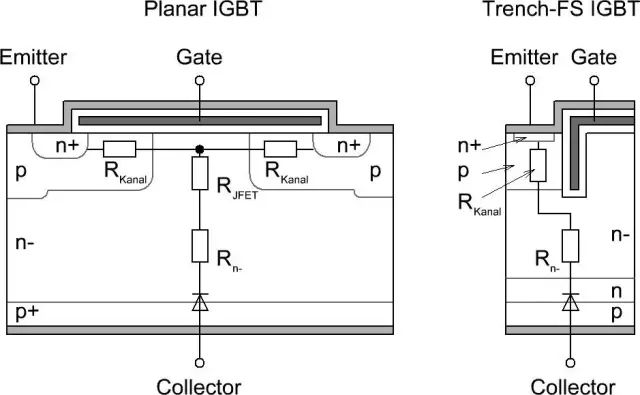
Figure 4. Comparison of on-state impedance between planar and trench-gate IGBTs.
The near-surface carrier concentration increases.
For planar gate IGBTs, the carrier concentration gradually decreases from the collector to the emitter. The design goal of new-generation IGBTs is to maintain a uniform distribution of carrier concentration between the collector and the emitter, preferably with a gradual increase. This can further reduce conduction losses without affecting tail current and turn-off losses. The figure below shows the carrier concentration distribution in the drift region of three different structures of IGBTs. We can see that near the emitter region, the carrier concentration in trench-gate IGBTs is much higher than that in planar gate IGBTs. Therefore, in trench-gate IGBTs, appropriate trench width and spacing can increase the carrier concentration in the near-surface layer of the N- region, thereby reducing the drift region resistance Rn-.
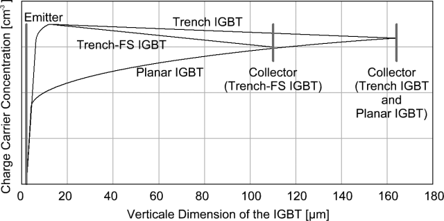
Figure 5. Carrier concentration distribution in an IGBT.
Increase in channel density
Compared to planar-gate IGBTs, the vertical structure of trench-IGBTs eliminates the area required for making conductive channels on the silicon surface, which allows for more compact cell designs. This means that more IGBT cells can be fabricated in the same chip area, resulting in wider conductive channels and lower channel resistance.
Despite the rapid rise of trench-IGBTs, planar-gate IGBTs still have their place. The first-movers are not being left behind because trench-IGBTs still have several challenges to overcome.
The technology for excavating smooth trench walls is difficult. The trench width of a typical trench-gate IGBT is only 1-2 μm, and the depth must reach 4-5 μm, or even deeper. The trenches are etched into the silicon surface using acid corrosion, and precise control of the trench width and depth is extremely difficult. Additionally, the trench walls must be as smooth and defect-free as possible, since uneven surfaces can impact breakdown voltage and reduce yield. The corners at the bottom of the trench must also be very smooth; otherwise, the electric field will concentrate at this point and seriously affect the voltage endurance. It is thus evident that trench-IGBT technology is much more difficult than planar-gate IGBT technology.
A wider conductive channel will increase the current during IGBT short-circuiting. As previously mentioned, the high channel density of trench-IGBTs reduces channel resistance, but one of its corresponding drawbacks is an increase in short-circuit current. In the worst case, the short-circuit current can be so large that it damages the IGBT in a very short amount of time. To make the IGBT capable of withstanding short circuits of up to 10 microseconds (under specified test conditions), the channel width and adjacent cells need to be designed very carefully, for example, by increasing the distance between cells to reduce the number of effective cells per single crystal. Another method is not to connect all gates to a common gate, but to short the gates of some cells with their emitter. This technique is called insert-merged-cell technology. By using this method, channel density can be reduced, thus reducing short-circuit current and enhancing the device's short-circuit capability.



Site Map | 萨科微 | 金航标 | Slkor | Kinghelm
RU | FR | DE | IT | ES | PT | JA | KO | AR | TR | TH | MS | VI | MG | FA | ZH-TW | HR | BG | SD| GD | SN | SM | PS | LB | KY | KU | HAW | CO | AM | UZ | TG | SU | ST | ML | KK | NY | ZU | YO | TE | TA | SO| PA| NE | MN | MI | LA | LO | KM | KN
| JW | IG | HMN | HA | EO | CEB | BS | BN | UR | HT | KA | EU | AZ | HY | YI |MK | IS | BE | CY | GA | SW | SV | AF | FA | TR | TH | MT | HU | GL | ET | NL | DA | CS | FI | EL | HI | NO | PL | RO | CA | TL | IW | LV | ID | LT | SR | SQ | SL | UK
Copyright ©2015-2025 Shenzhen Slkor Micro Semicon Co., Ltd