Service hotline
+86 0755-83044319
release time:2023-09-09Author source:SlkorBrowse:13329
Cars are posing higher demands
The automotive industry is another driving factor for semiconductor technology, including electric vehicles (EVs) and autonomous driving. In addition to advanced battery management systems, future cars will require next-generation sensor technologies, combining multiple multispectral cameras and multiple radars, including short-range and long-range radars. "All these sensors will generate an incredible amount of data," says Van den Hove. "To address this challenge, our cars will need a completely new computing architecture, running a large amount of artificial intelligence on powerful centralized electronic control units. As we transition from current Advanced Driver Assistance Systems (ADAS) to increasingly autonomous levels, the required computing power grows exponentially. The electronic control units in cars are actually evolving rapidly to match the performance levels of former supercomputers," he says.
He adds that while the semiconductor content in cars will significantly increase, leading to continuous growth in semiconductor demand, the total global production of cars has not increased significantly. "Designing these highly expensive computing systems on chips and optimizing them for specific markets such as high-end and low-end markets in a flexible manner is not straightforward," he says. "Therefore, we need to optimize these computing architectures while considering flexibility, complexity, energy efficiency, and affordability."
One approach that is generating interest in this regard is chiplet-based design, where the design is broken down into smaller silicon chiplets that are fused together using advanced heterogeneous integration technologies. "With chiplets, ECUs can be configured in a more flexible manner, allowing for high-end or low-end configurations without the need to redesign the entire chip. Since the chip will be smaller, it will enable the reuse of IP, which will provide better yield and reliability, which is crucial for the automotive industry," says Van den Hove.
Moore's Law, 2D scaling, 3D stacking, and chiplets
For decades, the semiconductor industry has enjoyed the benefits of two-dimensional scaling defined by Moore's Law. As the pace of this type of scaling slows down, alternative methods such as chip stacking and chiplets are coming into play. "We believe that Moore's Law in its traditional sense remains crucial. In fact, scaling based on feature size reduction of individual transistors is still one of the few technologies that can deliver true exponential growth in complexity," says Van den Hove.
He presented imec's roadmap for the next decade (Figure 4), which includes continuing with 2D scaling as well as introducing new technologies like forksheet transistors and complementary FET (CFET). In the CFET architecture, n and pMOS devices are stacked together, further maximizing the effective channel width. "By combining optical lithography-based scaling with the introduction of new interconnect schemes, new materials, and new device architectures like CFET, we can achieve several more generations of continued scaling," says Van den Hove.
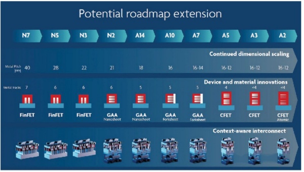
Figure 4
Van den Hove also discussed the "walls" that may be difficult to overcome. These include the power wall, where it becomes increasingly challenging to extend the power consumption for each transistor, and the memory wall, defined by the delay between the time a CPU needs data from cache or DRAM and the time it can access the data. "Due to the significant workload of artificial intelligence, effectively moving data into and out of our processors is becoming increasingly difficult. In fact, for specific AI workloads in high-performance computing, processors are only active less than 3% of the time," he said. "Most of the time, they are actually waiting for data, so we need to reconsider the memory system architecture."
Imec also identified three additional walls:
1. Scaling wall: The scaling speed enabled by pure optical lithography is slowing down. As the individual structures of microchips and transistors approach atomic sizes, quantum effects start to interfere with the operation of microchips, making scaling increasingly difficult.
2. Sustainability wall: The manufacturing of semiconductor devices adds to the environmental footprint, including greenhouse gas emissions, water consumption, natural resource usage, and energy consumption.
3. Cost wall: Clearly, as complexity increases, chip manufacturing costs, as well as the costs of design and process development, may experience explosive growth.
To be continued...



Site Map | 萨科微 | 金航标 | Slkor | Kinghelm
RU | FR | DE | IT | ES | PT | JA | KO | AR | TR | TH | MS | VI | MG | FA | ZH-TW | HR | BG | SD| GD | SN | SM | PS | LB | KY | KU | HAW | CO | AM | UZ | TG | SU | ST | ML | KK | NY | ZU | YO | TE | TA | SO| PA| NE | MN | MI | LA | LO | KM | KN
| JW | IG | HMN | HA | EO | CEB | BS | BN | UR | HT | KA | EU | AZ | HY | YI |MK | IS | BE | CY | GA | SW | SV | AF | FA | TR | TH | MT | HU | GL | ET | NL | DA | CS | FI | EL | HI | NO | PL | RO | CA | TL | IW | LV | ID | LT | SR | SQ | SL | UK
Copyright ©2015-2025 Shenzhen Slkor Micro Semicon Co., Ltd