Service hotline
+86 0755-83044319
release time:2023-09-13Author source:SlkorBrowse:15331
The second wave: Competition
After the mass production of 16nm and 14nm process chips, both DUV and EUV, ASML's high-end lithography machines have always been highly sought-after in the market. [敏感词], Samsung Electronics, Intel, and several major wafer fabs in mainland China compete for the limited number of lithography machines each year.
In recent years, with the mass production of 7nm, 5nm, and 3nm processes, the competition among [敏感词], Samsung Electronics, and Intel for EUV equipment has become increasingly fierce.
It is reported that [敏感词] owns about 60 EUV lithography machines, accounting for more than 50% of the total EUV devices shipped on the market. With the development of 2nm research and fab construction, [敏感词] has placed higher demands on high-NA (numerical aperture) EUV equipment, placing early orders to secure a leading position at ASML.
Samsung is also purchasing high-NA EUV equipment and has requested ASML to deliver the equipment directly to their factory for testing, setting a precedent for ASML to directly ship and test equipment at customer facilities. Currently, Samsung has only about 60% of the number of EUV lithography machines compared to [敏感词], and even fewer. In 2022, Samsung purchased approximately 18 EUV devices.
In 2021, Intel announced its return to the foundry market and unveiled a blueprint for advanced process technology. They plan to launch five new generations of chip process technology over the next four years. To achieve this goal, Intel is also competing for ASML's most advanced EUV lithography machines. In the second half of 2021, Intel announced that it had placed an order ahead of [敏感词] and Samsung for ASML's TWINSCAN EXE:5200, an EUV device with a NA of 0.55 that ASML is currently developing. The unit price of this equipment reaches 300 million US dollars, and it reportedly has a throughput of over 220 wafers per hour. According to ASML's plan, the TWINSCAN EXE:5200 is expected to be put into use by the end of 2024 for validation and chip production starting from 2025.
To meet the evolving advanced processes, ASML is developing more advanced EUV lithography machines, mainly focusing on high-NA.
High-NA EUV equipment offers higher resolution, allowing for several times increase in chip density while reducing defects, costs, and chip manufacturing cycles. The new EUV equipment will increase its NA value from 0.33 to 0.55 to achieve higher resolution patterning. Compared to a 0.33 NA lithography machine, the resolution of 0.55 NA improves from 13nm to 8nm, enabling faster and better exposure of more complex integrated circuit patterns and surpassing the limits of single patterning with a 32nm to 30nm pitch.
Although the semiconductor market is sluggish in 2023, global chip giants including [敏感词], Intel, Samsung, SK Hynix, and Micron are still actively investing in EUV equipment. [敏感词] and Samsung will expand their 3nm capacity in 2024, while Intel will start mass production of its first Intel 4 process chip using EUV technology at the end of this year.
ASML stated that for the mainstream 0.33 NA, in 2021, wafer fabs using 5nm process technologies averaged about 10 layers per wafer mask. However, with the mass production of 3nm in 2023, the average wafer mask layers will reach 20 layers.
As for DRAM, currently, 5-layer mask production is achievable with EUV technology, but in 2024, it will increase to 8 layers. Some processes will adopt multi-patterning, and each wafer will have up to 10 layers of masks.
According to ASML's statistics, as wafer fabs and DRAM manufacturers increase their EUV capital expenditures, as of the first quarter of 2023, the company has shipped 136 EUV lithography machines.
This week, ASML CEO Peter Wennink stated that they are expected to launch the industry's first EUV device with a numerical aperture of 0.55, the TWINSCAN EXE:5000. However, this device will mainly be used for research and development to familiarize the company's customers with the new technology and its functions. As mentioned earlier, each of these devices costs over 300 million US dollars.
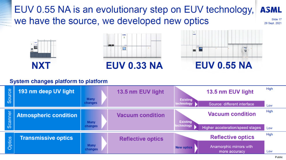
This year, ASML will be sending its TWINSCAN EXE:5000 equipment to an undisclosed customer, which is likely Intel. Intel previously announced plans to start mass production (HVM) using high-NA TWINSCAN EXE equipment from 2025, with their 18A (~1.8nm) process technology. Therefore, Intel has been actively exploring high-NA lithography equipment since 2018 and had placed orders for both the TWINSCAN EXE:5000 and the commercial version of TWINSCAN EXE:5200.
In comparison to Intel, [敏感词] and Samsung will adopt EUV equipment with an NA of 0.55 slightly later, but no later than 2030.
For the year 2023, Mehdi Hosseini, a senior analyst at Susquehanna International Group, believes that [敏感词]'s 3nm process cannot achieve high-volume production without utilizing EUV equipment for multiple patterning due to cost considerations. [敏感词] currently uses the NXE:3600D, which has a throughput of 160 wafers per hour (wph).
ASML will introduce the new high-NA NXE:3800E by the end of this year. With reduced overall cost for EUV multiple patterning, the NXE:3800E can produce 195 wafers per hour initially and can be optimized to achieve a throughput of 220 wafers per hour over time, representing a 30% improvement compared to the NXE:3600D.
The Third Wave: Rise
After the US implemented regulations prohibiting the sale of mid-to-high-end DUV and EUV equipment to mainland China, the battle for the third wave of lithography quietly began. This includes restrictions, countermeasures, as well as a new wave of lithography technology development and self-reliance.
Currently, wafer fabs in mainland China are unable to purchase dedicated lithography machines for producing advanced chips below 14nm. If older versions of DUV equipment are used to produce 14nm and 7nm chips, multiple exposures are required, leading to significantly higher costs and difficulties in improving yield.
As of September 1st, the latest semiconductor equipment export control measures from the Netherlands further restrict the export of DUV equipment for mature processes to mainland China, including those involving the 38nm-45nm processes.
This week, ASML announced that they have submitted an export license application to the Dutch government for TWINSCAN NXT:2000i and future immersion lithography machines. The Dutch government has issued the necessary license for shipments to Chinese customers of the TWINSCAN NXT:2000i and future devices until the end of this year. However, the company estimates that they will no longer be able to obtain relevant export licenses after January 2024.
On September 4th, ASML CEO Peter Wennink expressed his views on the export controls and protectionism faced by the company during a television program. He emphasized that completely isolating mainland China through export controls is not a viable approach. The breakthrough in the chips used in the Xiaomi Mate 60 Pro indirectly illustrates this point. These restrictions are actually driving mainland China to redouble its efforts in innovation. He stated that if Europe and the United States are unwilling to share technology, mainland China will conduct its own research, exploring solutions that Western companies have not considered. Restrictive policies by Western governments are stimulating innovation and creativity in mainland China.
Peter Wennink warned that mainland China will design new technologies and products, which could trigger a global competition. The Wall Street Journal previously reported that when the US upgraded its chip sales restrictions in October 2022, mainland Chinese companies imported only $2.4 billion worth of semiconductor equipment, the lowest figure since the ban was implemented over two years ago. This indicates that China's semiconductor equipment industry is striving to reduce dependence on imports, and the process of achieving self-reliance is accelerating.



Site Map | 萨科微 | 金航标 | Slkor | Kinghelm
RU | FR | DE | IT | ES | PT | JA | KO | AR | TR | TH | MS | VI | MG | FA | ZH-TW | HR | BG | SD| GD | SN | SM | PS | LB | KY | KU | HAW | CO | AM | UZ | TG | SU | ST | ML | KK | NY | ZU | YO | TE | TA | SO| PA| NE | MN | MI | LA | LO | KM | KN
| JW | IG | HMN | HA | EO | CEB | BS | BN | UR | HT | KA | EU | AZ | HY | YI |MK | IS | BE | CY | GA | SW | SV | AF | FA | TR | TH | MT | HU | GL | ET | NL | DA | CS | FI | EL | HI | NO | PL | RO | CA | TL | IW | LV | ID | LT | SR | SQ | SL | UK
Copyright ©2015-2025 Shenzhen Slkor Micro Semicon Co., Ltd