Service hotline
+86 0755-83044319
release time:2023-09-13Author source:SlkorBrowse:12077
Looking at the historical development, the evolution and application of lithography machines (specifically referring to those used in the front-end processes of integrated circuit manufacturing) have encountered many twists and turns. Overall, there are two noteworthy periods. The first is when ASML emerged as a dominant player by leveraging immersion technology, surpassing the previous industry leaders. This was a battle of technologies. The second period began with the commercialization of extreme ultraviolet (EUV) lithography, as the competition for advanced process nodes (starting from 16nm) intensified among [敏感词], Samsung, and Intel, who vied for the limited EUV capacity. This was a battle of businesses.
From the current situation, the third wave of competition in lithography machines is brewing, and it is expected to be more complex and intense than the previous two waves.
The first wave: Counterattack
In 1957, Jay Lathrop and James Nall from a laboratory of the US Army patented the photolithography technology, which was used to deposit metal strips on ceramic substrates to connect discrete transistors. In 1959, Lathrop joined Texas Instruments and Nall went to Fairchild Semiconductor. In 1958, Jay Last and Robert Noyce manufactured the first "step-and-repeat" camera at Fairchild Semiconductor, using photolithography to make many transistors on a single wafer. This was the prototype of the photolithography machine.
In the 1980s, GCA Corporation from the United States had dominated the global photolithography machine market. However, due to the rush to deliver equipment to customers without proper inspection, hundreds of defective lenses were sent to the market. At almost the same period, Nikon from Japan improved the focusing system of the photolithography machine and developed g-line objectives with a larger numerical aperture, which allowed the system to project tiny patterns onto the photoresist more clearly. This innovation quickly allowed Nikon to dominate the market, and customers abandoned GCA's photolithography machines, causing GCA to decline rapidly.
At the same time, Canon also launched market-approved products, becoming one of the two leaders in the photolithography machine industry at that time alongside Nikon.
Meanwhile, based on its success in step-and-scan photolithography machines, ASML gradually caught up, especially with its iconic product PAS 5500, which was highly praised by the market. After years of hard work, ASML became a giant in the step-and-scan photolithography machine era.
However, at that time, ASML's industry position was not as prominent as it is now, and it was slightly inferior to Nikon and Canon.
ASML's dominance in the photolithography machine industry originated from the process upgrade from 193nm to 157nm. Before that, step-and-scan photolithography machines used the dry (exposure medium is air) technology route and supported technological advancement by using higher-level exposure light sources. In pursuit of higher resolution, the wavelength of the light source changed from the initial 365nm to 248nm, then to 193nm. After that, it was difficult to continue along this technological route.
At that time, the industry faced two choices: technological improvement and disruption. The two giants Nikon and Canon chose to improve their existing technological path, while ASML chose to take a gamble because a new immersion technology had emerged.
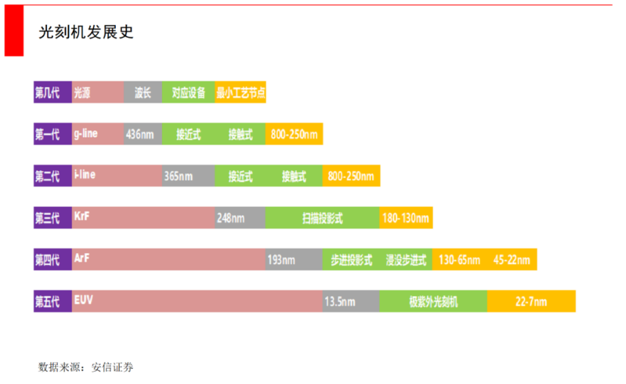
Immersion lithography, proposed by Benjamen Lin at the time when he was a scientist at [敏感词], creatively used water as the immersion medium. It still used the original 193nm wavelength light source, but through the refraction of water, the wavelength entering the photoresist was reduced to 134nm. The refractive index of a 193nm light source in air is 1, while it is 1.4 in water. This means that under the same light source conditions, the resolution of immersion lithography machines can be improved by 1.4 times.
However, this technology seemed too bold at the time, with high technical difficulties and costs. The beneficiaries of traditional lithography technologies were reluctant to accept it. Lin traveled to the United States, Japan, Germany, and the Netherlands to promote immersion lithography and sell his idea to lithography machine manufacturers. But he faced rejection from most industry giants, and Nikon even pressured [敏感词] to "kill" him.
In this situation, Lin placed his last hope on ASML, and the latter did not let him down. When technology and industry development reached a crossroads, ASML chose disruptive innovation and won the gamble.
In 2003, ASML and [敏感词] cooperated to develop the first immersion lithography equipment, the TWINSCAN XT:1150i, which was followed by an improved version the following year. In the same year, Nikon, with slow progress in research and development, finally introduced a prototype of a 157nm dry lithography machine.
One was the new technology that used the original 193nm light source and evolved to a wavelength of 132nm through water, while the other was a prototype with a wavelength of 157nm. The advantages of immersion lithography were evident. This technology became the mainstream lithography solution for subsequent process nodes such as 65nm, 32nm, 16nm, and 7nm, up until the current 3nm node.
Choice is greater than effort. ASML made the right choice, while Nikon and Canon made the wrong ones. The market quickly embraced immersion lithography machines, leaving the traditional dry lithography products sitting in warehouses gathering dust. This caused Nikon and Canon's billions of dollars in research and development expenses to go down the drain and their market share to decline significantly. In the 15 years before 2000, ASML was the smallest player in the top tier of lithography machines, with a market share of less than 10%. With the commercialization of immersion lithography, by 2008, ASML's market share reached 60%, standing out alone.
The first wave of technology-driven lithography machine competition ended, and ASML emerged as the winner.
To be continued...



Site Map | 萨科微 | 金航标 | Slkor | Kinghelm
RU | FR | DE | IT | ES | PT | JA | KO | AR | TR | TH | MS | VI | MG | FA | ZH-TW | HR | BG | SD| GD | SN | SM | PS | LB | KY | KU | HAW | CO | AM | UZ | TG | SU | ST | ML | KK | NY | ZU | YO | TE | TA | SO| PA| NE | MN | MI | LA | LO | KM | KN
| JW | IG | HMN | HA | EO | CEB | BS | BN | UR | HT | KA | EU | AZ | HY | YI |MK | IS | BE | CY | GA | SW | SV | AF | FA | TR | TH | MT | HU | GL | ET | NL | DA | CS | FI | EL | HI | NO | PL | RO | CA | TL | IW | LV | ID | LT | SR | SQ | SL | UK
Copyright ©2015-2025 Shenzhen Slkor Micro Semicon Co., Ltd