Service hotline
+86 0755-83044319

release time:2022-03-17Author source:SlkorBrowse:10681

Basic Semiconductors:
Headquarters project contract
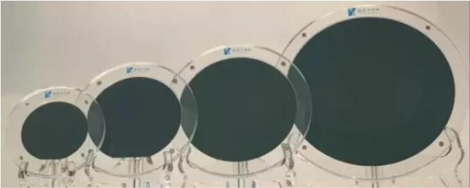
According to reports, the basic semiconductor contract constructionVehicle grade The third-generation semiconductor R&D and manufacturing headquarters project. In addition to this project, Basic Semiconductor has 3 production lines under construction: ▲Nanjing Pukou The manufacturing base has started construction in March 2020 and is expected to be connected by the end of 2021.
Process development and manufacturing of SiC epitaxial wafers; ▲Co-built by Yizhuang, Beijing6-inch silicon carbide wafer production line will achieve mass production in the fourth quarter of this year; ▲The third-generation semiconductor industry base in Shenzhen Pingshan has started construction at the end of 2020 and is expected to be put into production in 2023, with an annual production capacity will reach2 million SiC devices.
In addition to this project, Basic Semiconductor has 3 production lines under construction: ▲Nanjing Pukou The manufacturing base has started construction in March 2020 and is expected to be connected by the end of 2021.
Process development and manufacturing of SiC epitaxial wafers; ▲Co-built by Yizhuang, Beijing6-inch silicon carbide wafer production line will achieve mass production in the fourth quarter of this year; ▲The third-generation semiconductor industry base in Shenzhen Pingshan has started construction at the end of 2020 and is expected to be put into production in 2023, with an annual production capacity will reach2 million SiC devices.
Crystal Semiconductor:
GaN epitaxy project settled
At the same time, Jingzhan Semiconductor'sGallium nitride epitaxial materials R&D and industrialization projects were also signed and settled in Wuxi. Specific project information is yet to be announced. In addition to this project, in March 2021, Suzhou Industrial Park also announced the "Environmental Assessment Document for Jingzhan Semiconductor's New Gallium Nitride Epitaxial Wafer Production and Expansion Project". The project intends to invest250 million yuan, with an annual output of GaN epitaxial wafers after completion500,000 pieces . According to Jingzhan's official website, at the end of 2014, Jingzhan took the lead in releasing commercial 8-inch silicon-based nitride for the first time in the world Gallium epitaxial wafer products. Up to now, Jingzhan has completed the A+ round of financing to expand the production scale. The monthly production capacity of 150mm GaN-on-Si epitaxial wafers reaches10,000 pieces . At present, Jingzhan has more than 150 well-known semiconductor companies and research institute customers around the world. And not long ago, Jingzhan Semiconductor also showed a 12-inch, 1200V silicon-based GaN epitaxial wafer, which is the most suitable for the use of mainstream12-inch CMOS production line paved the way for GaN HEMT transistors.
Disclaimer: This article is reproduced from "The Third Generation Semiconductor Trend". This article only represents the author's personal views, not the views of Sac Micro and the industry, and is only for reprinting and sharing , support the protection of intellectual property rights, please indicate the original source and author for reprinting, if there is any infringement, please contact us to delete it.


Site Map | 萨科微 | 金航标 | Slkor | Kinghelm
RU | FR | DE | IT | ES | PT | JA | KO | AR | TR | TH | MS | VI | MG | FA | ZH-TW | HR | BG | SD| GD | SN | SM | PS | LB | KY | KU | HAW | CO | AM | UZ | TG | SU | ST | ML | KK | NY | ZU | YO | TE | TA | SO| PA| NE | MN | MI | LA | LO | KM | KN
| JW | IG | HMN | HA | EO | CEB | BS | BN | UR | HT | KA | EU | AZ | HY | YI |MK | IS | BE | CY | GA | SW | SV | AF | FA | TR | TH | MT | HU | GL | ET | NL | DA | CS | FI | EL | HI | NO | PL | RO | CA | TL | IW | LV | ID | LT | SR | SQ | SL | UK
Copyright ©2015-2025 Shenzhen Slkor Micro Semicon Co., Ltd
