Service hotline
+86 0755-83044319

release time:2022-03-17Author source:SlkorBrowse:12902
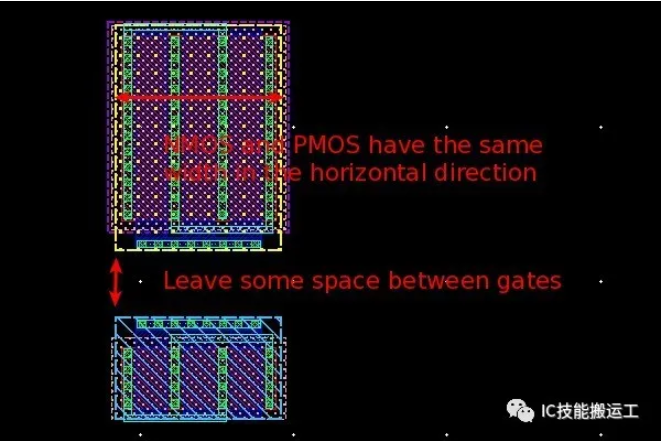
The devices with adjusted size and layout are shown in the figure. Next, start connecting devices, select M1 in LWS column, then use shortcut key P or R to complete the connection between MOS tubes, reserve the lines of AVDD and AVSS at the upper and lower positions respectively, and finally use shortcut key L to name the connection nodes (use txt layer corresponding to metal, for example, M1TXT layer). After completing the above steps, the layout should look similar to the screenshot below.
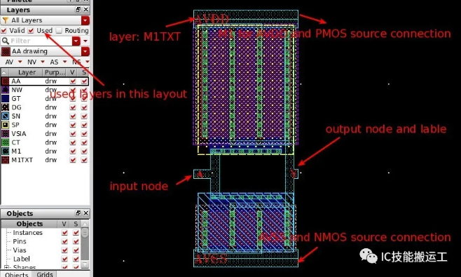
After completing the above steps, you can select: Edit->Advanced->Move Origin in the layout design interface, and select the coordinate origin of the layout, which will be more convenient when you need to call it later.
Disclaimer: This article is reproduced from "EETOP". This article only represents the author's personal views, and does not represent the views of Sacco Micro and the industry. It is only for reprinting and sharing to support the protection of intellectual property rights. Please indicate the original source and author when reprinting. If there is any infringement, please contact us to delete it.
Company Tel: +86-0755-83044319
Fax/fax:+86-0755-83975897
Email: 1615456225@qq.com
QQ: 3518641314 Manager Li
QQ: 332496225 Manager Qiu
Address: Room 809, Block C, Zhantao Technology Building, No.1079 Minzhi Avenue, Longhua New District, Shenzhen


Site Map | 萨科微 | 金航标 | Slkor | Kinghelm
RU | FR | DE | IT | ES | PT | JA | KO | AR | TR | TH | MS | VI | MG | FA | ZH-TW | HR | BG | SD| GD | SN | SM | PS | LB | KY | KU | HAW | CO | AM | UZ | TG | SU | ST | ML | KK | NY | ZU | YO | TE | TA | SO| PA| NE | MN | MI | LA | LO | KM | KN
| JW | IG | HMN | HA | EO | CEB | BS | BN | UR | HT | KA | EU | AZ | HY | YI |MK | IS | BE | CY | GA | SW | SV | AF | FA | TR | TH | MT | HU | GL | ET | NL | DA | CS | FI | EL | HI | NO | PL | RO | CA | TL | IW | LV | ID | LT | SR | SQ | SL | UK
Copyright ©2015-2025 Shenzhen Slkor Micro Semicon Co., Ltd
