+86 755-83044319

Technical Blogs

/
/

Simulation integrated circuit design process -layout design basis (1)

release time:2022-03-17Author source:SlkorBrowse:2203

In analog circuit design, besides circuit design and simulation, layout design is also a very important content. The quality of layout design is directly related to the performance of the chip. In the next few times, we will learn the content of layout design with you.

Preparation before layoutHow is the circuit designed on the software processed into a chip with certain functions in the foundry? The circuit design is connected with the chip through layout, the circuit design is only a form, and the layout is the concrete expression of the circuit. Generally speaking, the foundry is to manufacture the mask according to the layout provided by the designer, and then realize the chip manufacturing by combining the shape of the mask with the technological process.

Cross-sectional view of inverter, the distribution of areas in the figure determines the areas of NMOS and PMOS. Layout design is to determine how these areas are distributed and how the connection between NMOS and PMOS is realized.After knowing what the layout does, we will go back to a question left before: How does PDK contain process information?It's not easy to talk about this problem in depth. You can't understand it at first, but you will gradually become familiar with it with the in-depth study of the technological process in the future. Here's a little explanation. Look at it as a popular science, and the content is not necessarily rigorous. Please don't delve into it.
 
  First of all, the factory has a definition of the process used in PDK. This file is called techfile.tf You can look it up in your own PDK, and you should all find this file. In this file, the names, display colors, etc. of each layer used in the process are defined. Besides, each layer will correspond to a numerical number. You can make an analogy like this:A processing layer in the craft is like a person, the name of the layer corresponds to the person's name, the display color of the layer corresponds to the person's clothes, and the number of the layer corresponds to the person's ID number. Daily communication between people only needs to know the person's name and what kind of clothes he wears, and he doesn't care about his ID number. Only when verifying a person's identity, he needs to provide his ID number.In layout design, the designer also sees the name and color of each layer, and won't tangle with the number of the corresponding layer, because that number is used by the craft factory to determine which processing step this layer corresponds to specifically, and it is not closely related to the designer.Of course, the actual PDK will compile the techfile.tf file, make it into something that can't be edited at will, and then provide it to users. Otherwise, if users change the content of techfile.tf at least, then the process information in PDK will change, and the factory can't confirm the process during processing!PDK will provide users with a display file named: display.drf while providing process information. This file defines "clothes" of different process layers. Just as a person's ID number can't be changed, but no one interferes with what kind of clothes to wear. The factory won't let users change the corresponding number of each floor, but how to display each floor depends on the user's habits. Users can modify the contents of the display.drf file and change the display color and display method of the floor. This file can also be found in PDK, so you can open it and read the contents.Before starting the layout, it is necessary to declare to the software which process is adopted in this design. Remember when we created a new design library, we skipped a process-related step? It's time to determine the design process here.  
 In the CIW window, select: Tools-> Technology File Manager-> Attach, and then in the pop-up box, select to associate your design library with the process library provided by PDK, as shown in the figure below. This step can also be implemented when creating a new library.


  In addition, in order to ensure that the layout display file is consistent with the techfile.tf file of PDK, it is necessary to copy the display.drf file in PDK to the startup directory of Cadence software before starting the layout.In some processes, the display.drf file may be related to the display of the schematic diagram. If any incorrect display such as wiring is found in the schematic diagram, you can copy the display.drf file in the process library to the working directory first, and then consider other reasons. Familiar with layout design environmentFirst, learn about layout design tools, and at the same time, learn about layout design by opening the device layout provided in PDK. Find the library provided by PDK in the software Library Manager window, select the device that provides layout View, and open the corresponding layout.


The library used by primary school students is smic18mmrf. Select device n33 and open the corresponding layout, as shown in the following figure. 

Check the device layout provided in PDK.      

图片

Introduction to NMOS layout and software interface. Slide up and down to see more content! On the left side of the layout interface, there is a window for displaying process layers (LSW), which is the most frequently used window during layout drawing. In it, you can set the selection of a certain layer, which layers to display and which layers can be selected, and you can also change the display shape and color of layers.At the top of the layout interface is the toolbar, which is similar to the schematic interface, including creating new content, calling devices and so on. In addition, it is the layout work area, where the user calls and draws the layout.

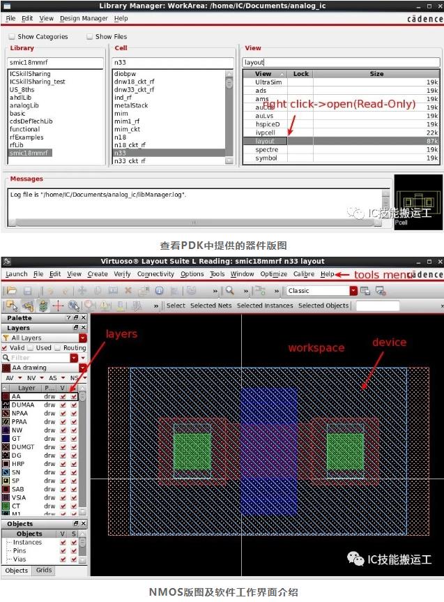
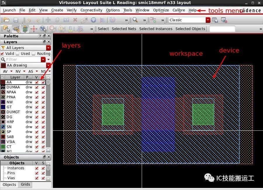
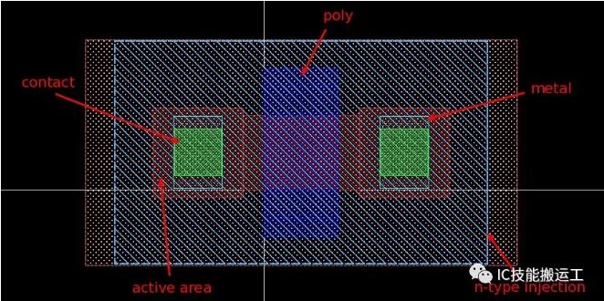
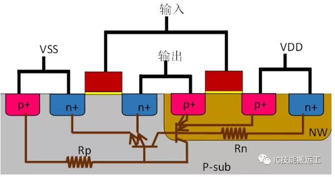
Combine the above layout example with the cross-sectional view of CMOS inverter given at the beginning of this paper to get a preliminary understanding of the layout, and at the same time get familiar with some common names of some layers in the layout.The name and significance of common layers in layout

习惯叫法

实现功能

显示名称(smic18mmrf)

poly

定义MOS管的栅极或者电阻区域等

GT

metal

所有金属互连

M1、M2、M3...

active area

定义离子注入区域

AA

n plus(p plus)

定义离子注入类型

SN(SP)

contact

active area(poly)与M1的过孔

CT

via

金属之间的过孔

V1、V2、V3...

Swipe up and down,
left and right to see more content!
There are also many shortcut keys in the use of layout tools to improve work efficiency. Here are some common shortcut keys, and users can try the functions of each shortcut key by themselves.Common shortcut keys in layout design

快捷键

实现功能

快捷键

实现功能

p

创建连线

shift+p

创建多边形

r

创建矩形

shift+r

改变已有形状

o

[敏感词]过孔

shift+o

旋转工具

i

[敏感词]实例

q

编辑属性

c

复制图形

shift+c

裁剪工具

m

移动工具

shift+m

合并图形

l

创建线名

s

拉伸工具

k

创建标尺

shift+k

清除标尺

f

显示全部

n

45°走线

u

撤销操作

shift+u

取消撤销操作

t

查看层名

z

区域放大

y

复制区域

shift+y

粘贴区域

v

绑定图形

backspace

撤销一次操作

a

快速对齐

shift+a

区域选择

ctrl+z

放大

shift+z

缩小

ctrl+f

显示层次

shift+f

铺平显示

x

原地编辑

shift+x

进入下一级

ctrl+b

返回上一级

ctrl+a

选中所有

ctrl+w

关闭视图

shift+w

下一个视图

tab

移动视图

delete

删除内容

enter

完成操作

esc

结束操作

方向键

移动视角

shift+方向键

移动光标

Swipe up and down, left and right to see more content!

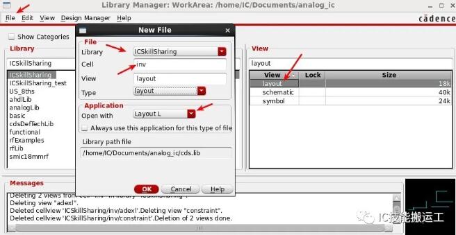
These are the shortcut keys in the default state of some software. After getting familiar with them, users can change the shortcut keys according to their own operating habits. There may be some translation deviation in the function of shortcut keys. I hope you can experience it slowly in practice. Skilled use of shortcut keys can greatly improve layout efficiency. Inverter layout designCreate a layout View of the inverter. In the Library Manager interface: File->New->Cell View, select your own engineering library, select INV for cell, and Layout for type. Open the tool and select the default. After confirmation, the layout design window will pop up.


  There are different ways to realize the layout of devices in layout design:

User-drawn device layout: according to the definition of device in process and the size of device in design, draw all layers in the device layer by layer to realize the function of the device (applicable to the design without PDK).

Call the device in PDK: Call the device provided by the process library from PDK, and you can easily change the device size (applicable to PDK-based design).Importing devices from schematic diagram: The software supports importing device layout from schematic diagram, and the attributes of imported devices are consistent with those in schematic diagram (applicable to PDK-based design).


Because we are based on the layout design of PDK, we can directly use the device layout provided by PDK, thus avoiding the trouble of designing the device layout ourselves.


Use the shortcut key I in the layout design interface, and then call the device similar to that in schematic design, but at this time, select the device View as layout, then fill in the device parameters, and put the called device in the work area, such as calling an n33 NMOS.  


Disclaimer: This article is reproduced from "EETOP". This article only represents the author's personal views, and does not represent the views of Sacco Micro and the industry. It is only for reprinting and sharing to support the protection of intellectual property rights. Please indicate the original source and author when reprinting. If there is any infringement, please contact us to delete it.

Company Tel: +86-0755-83044319
Fax/fax:+86-0755-83975897
Email: 1615456225@qq.com
QQ: 3518641314 Manager Li
QQ: 332496225 Manager Qiu
Address: Room 809, Block C, Zhantao Technology Building, No.1079 Minzhi Avenue, Longhua New District, Shenzhen


Service hotline

+86 0755-83044319

Hall Effect Sensor

Get product information

WeChat

WeChat