Service hotline
+86 0755-83044319

release time:2022-03-17Author source:SlkorBrowse:10744
Most digital-to-analog converters (DACs) work with a fixed positive reference voltage, and the output voltage or current is proportional to the product of the reference voltage and the set digital code. However, for the so-called multiplying digital-to-analog converter (MDAC), this is not the case. Its reference voltage can be changed, and the range of change is usually ± 10 V。
Therefore, the analog output can be influenced by the reference voltage and digital code (both of which are dynamic).applyWith the help of corresponding wiring, the module can output amplified, attenuated or inverted signals (relative to the reference signal). Therefore, its application fields include waveform generator, programmable filter and PGA (Programmable Gain Amplifier), and many other applications where the offset or gain must be adjusted.
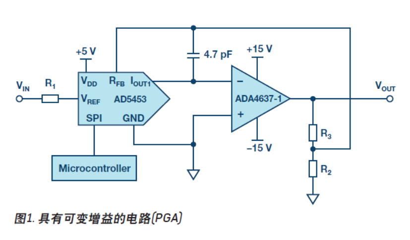
Figure 1 shows a 14-bit MDAC AD5453 with a downstream amplifier, which can amplify or attenuate the signal according to the programmed digital code of the DAC.
Circuit calculation
The output voltage (VOUT) of this circuit is calculated as follows:
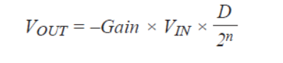
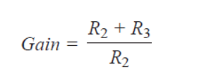
Besides the gain and the set digital code D of DAC, the output voltage is also affected or limited by the power supply voltage of operational amplifier. In the case shown, the power supply voltage of ADA4637-1 amplifier is ± 15 V voltage, should output ± The maximum voltage of 1V, so its control range is large enough. The gain is determined by resistors R2 and R3:
All resistors (R1 to R3) should have the same temperature coefficient of resistance (TCR), but not necessarily the same as the TCR of the internal resistor of DAC. R1 is used to adjust the internal resistance (RFB) of DAC according to R2 and R3 and the following relationship:
R1 + RFB = RFB + R2 || R3
R1 = R2 || R3
When selecting resistors, it is necessary to ensure that the operational amplifier is still in the working range at the maximum input voltage (DAC can process at VREF ± 10 V )。 It should also be noted that the input bias current (IBIAS) of the amplifier will be amplified by the resistor (RFB+R2 || R3), which has considerable influence on the offset voltage. It is for this reason that the operational amplifier ADA4637-1 with ultra-low input bias current and ultra-low input offset voltage (according to the data sheet) is selected. To prevent the instability of the closed-loop control system or the so-called ringing, insert a 4.7 pF capacitor between IOUT and RFB; This method is especially recommended for fast amplifiers.
As mentioned earlier, the offset voltage of the amplifier will be amplified by the closed-loop gain. When the external resistance for setting the gain changes, and the change value corresponds to the digital step size, this value will increase to the expected value, resulting in differential nonlinear error. If it is large enough, it may lead to non-monotonic DAC behavior. To avoid this effect, it is necessary to choose an amplifier with low offset voltage and low input bias current.Compared with the advantages of other circuitsIn principle, if an external reference is allowed, standard DAC can also be used, but there are some important differences between standard DAC and MDAC. The reference input of standard DAC can only handle unipolar voltage with limited amplitude. Besides amplitude, the reference input bandwidth is also very limited. This is indicated in the data sheet by the multiplication bandwidth value. Taking the AD566416-bit DAC as an example, the value is 340 kHz. The reference input of the multiplying DAC can use bipolar voltage, which can also be higher than the power supply voltage. The bandwidth is also much higher—the typical bandwidth of the ——AD5453 is 12 MHz.tag
Multiplicative DAC is not widely used, but it offers many possibilities. In addition to the self-made PGA with high bandwidth, the mobile application is also a very suitable application, because its power consumption requirement is lower than 50μ W.
Disclaimer: This article is reproduced from "Electronic Planet 2021". This article only represents the author's personal views, and does not represent the views of Sacco Micro and the industry. It is only for reprinting and sharing to support the protection of intellectual property rights. Please indicate the original source and author when reprinting. If there is any infringement, please contact us to delete it.
Company Tel: +86-0755-83044319
Fax/fax:+86-0755-83975897
Email: 1615456225@qq.com
QQ: 3518641314 Manager Li
QQ: 332496225 Manager Qiu
Address: Room 809, Block C, Zhantao Technology Building, No.1079 Minzhi Avenue, Longhua New District, Shenzhen


Site Map | 萨科微 | 金航标 | Slkor | Kinghelm
RU | FR | DE | IT | ES | PT | JA | KO | AR | TR | TH | MS | VI | MG | FA | ZH-TW | HR | BG | SD| GD | SN | SM | PS | LB | KY | KU | HAW | CO | AM | UZ | TG | SU | ST | ML | KK | NY | ZU | YO | TE | TA | SO| PA| NE | MN | MI | LA | LO | KM | KN
| JW | IG | HMN | HA | EO | CEB | BS | BN | UR | HT | KA | EU | AZ | HY | YI |MK | IS | BE | CY | GA | SW | SV | AF | FA | TR | TH | MT | HU | GL | ET | NL | DA | CS | FI | EL | HI | NO | PL | RO | CA | TL | IW | LV | ID | LT | SR | SQ | SL | UK
Copyright ©2015-2025 Shenzhen Slkor Micro Semicon Co., Ltd
