Service hotline
+86 0755-83044319

release time:2022-03-17Author source:SlkorBrowse:12988
The MOSFET selection of DC/DC switching controller is a complicated process. Only considering the rated voltage and current of MOSFET is not enough to select a suitable MOSFET. To keep MOSFET within the specified range, a balance must be struck between low gate charge and low on-resistance. In a multi-load power supply system, this situation will become more complicated.

Figure 1-Schematic diagram of step-down synchronous switching regulator
DC/DC switching power supply is widely used in many modern electronic systems because of its high efficiency. For example, a step-down synchronous switching regulator with a high-side FET and a low-side FET is shown in Figure 1. The two FETs will switch according to the duty ratio set by the controller, aiming to achieve the ideal output voltage. The duty cycle equation of the voltage regulator is as follows:
1) duty cycle (high side FET, upper tube) = Vout/(Vin* efficiency)
2) Duty cycle (low side FET, lower tube) = 1–DC (high side FET)
The FET may be integrated into the same chip as the controller, thus realizing the simplest solution. However, in order to provide high current capability and/or achieve higher efficiency, FET needs to always be an external component of the controller. In this way, the maximum heat dissipation capacity can be achieved, because it physically isolates the FET from the controller, and it has the maximum flexibility of FET selection. Its disadvantage is that the FET selection process is more complicated, because there are many factors to consider.
A common question is "Why don't you let this 10A FET also be used in my 10A design?" The answer is that this 10A rated current is not suitable for all designs.
Factors to be considered when selecting FET include rated voltage, ambient temperature, switching frequency, controller driving capability and heat dissipation component area. The key point is that if the power consumption is too high and the heat dissipation is insufficient, the FET may overheat and catch fire. We can estimate the junction temperature of a FET by using the package/heat dissipation component ThetaJA or thermistor, FET power consumption and ambient temperature. The specific method is as follows:
3) Tj = ThetaJA * FET power consumption (PdissFET)+ambient temperature (Tambient)It requires calculating the power consumption of FET. This power consumption can be divided into two main parts: AC and DC losses. These losses can be calculated by the following equation:
4) AC loss: AC power consumption (PswAC) = ½ * Vds * Ids * (trise + tfall)/Tsw
In which Vds is the input voltage of the high-side FET, Ids is the load current, trise and tfall are the rise time and fall time of the FET, and Tsw is the switching time (1/ switching frequency) of the controller.
In which RdsOn is the on-resistance of FET, and Iout is the load current of buck topology.
Other causes of loss include output parasitic capacitance, gate loss, and body diode loss caused by conduction of low-side FET during dead time, but in this paper, we will mainly discuss AC and DC losses.
When the switching voltage and current are both non-zero, AC switching loss occurs during the transition period between on and off of the switch. The highlight in Figure 2 shows this situation. According to equation 4), one way to reduce this loss is to shorten the rise time and fall time of the switch. This goal can be achieved by selecting a FET with lower gate charge. Another factor is the switching frequency. The higher the switching frequency, the greater the percentage of switching time spent in the lifting transition region shown in fig. 3. Therefore, higher frequency means greater AC switching loss. Therefore, another way to reduce AC loss is to reduce the switching frequency, but this requires a larger and usually more expensive inductor to ensure that the peak switching current does not exceed the specification.
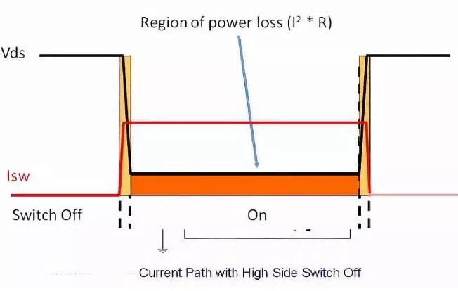
Figure 2-AC Loss Diagram
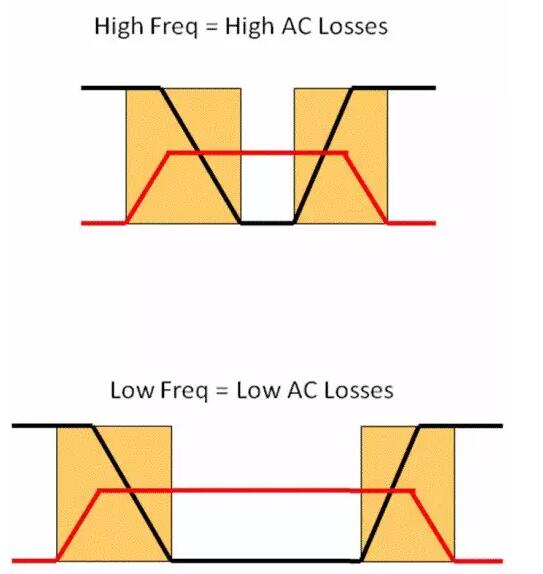
Figure 3-Influence of switching frequency on AC loss
When the switch is on, DC loss occurs, which is due to the on-resistance of FET. This is a very simple I2R loss formation mechanism, as shown in Figure 4. However, the on-resistance changes with the junction temperature of FET, which makes this situation more complicated. Therefore, when using equations 3), 4) and 5) to calculate the on-resistance accurately, it is necessary to use the iterative method and consider the temperature rise of FET.
The simplest way to reduce DC loss is to choose a FET with low on-resistance. In addition, the DC loss is directly proportional to the percentage conduction time of the FET, which is the duty cycle of the high-side FET controller plus 1 minus the duty cycle of the low-side FET, as mentioned above. As we can know from fig. 5, longer on-time means greater DC switching loss, so the DC loss can be reduced by reducing on-time /FET duty cycle. For example, if an intermediate DC voltage rail is used and the input voltage can be modified, the designer may be able to modify the duty cycle.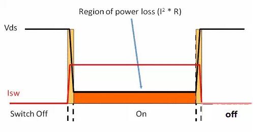
Figure 4-DC Loss Diagram
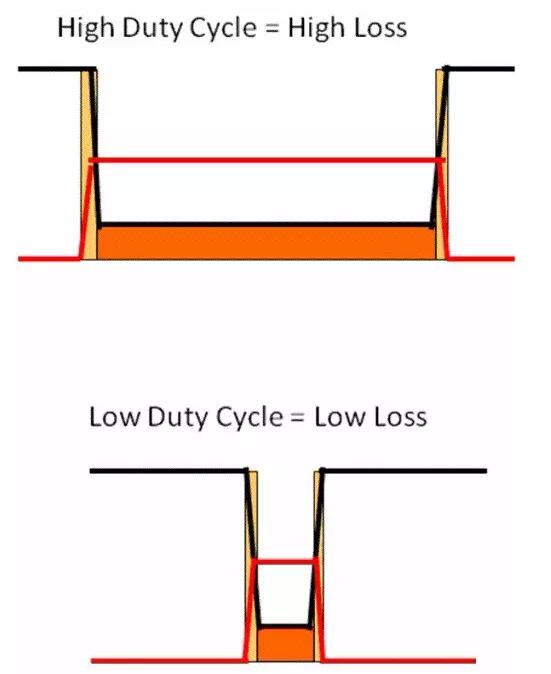
Figure 5-Effect of Duty Cycle on DC Loss
Although it is a simple solution to choose a FET with low gate charge and low on-resistance, some compromises and balances need to be made between these two parameters. Low gate charge usually means smaller gate area/fewer parallel transistors, and the resulting high on-resistance. On the other hand, using larger/more parallel transistors generally leads to low on-resistance, which leads to more gate charges. This means that FET selection must balance these two conflicting specifications. In addition, the cost factor must also be considered.
Low duty cycle design means high input voltage. For these designs, the high-side FET is turned off most of the time, so the DC loss is low. However, high FET voltage brings high AC loss, so FET with low gate charge can be selected, even if the on-resistance is high. Low-side FET is always on, but the AC loss is minimal. This is because the voltage of the low-side FET during on/off is very low due to the FET body diode. Therefore, it is necessary to select a low on-resistance FET, and the gate charge can be high. Figure 7 shows the above situation.
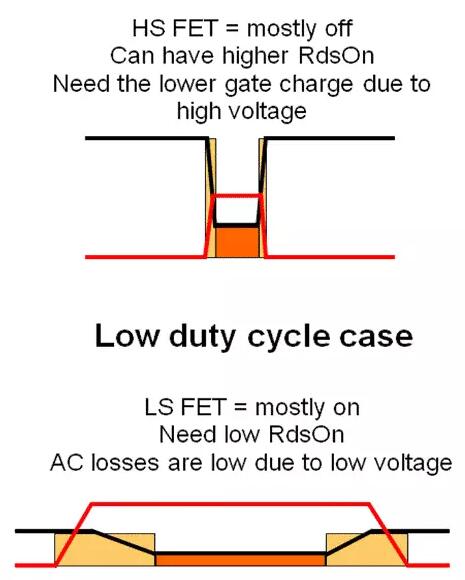
Figure 7— Power Consumption of High-side and Low-side FET with Low Duty Cycle Design
If we lower the input voltage, we can get a high duty cycle design, in which the high-side FET is on most of the time, as shown in Figure 8. In this case, the DC loss is high, and low on-resistance is required. According to different input voltages, AC loss may not be as important as that of low-side FET, but it is still not as low as that of low-side FET. Therefore, an appropriate low gate charge is still required. This requires a compromise between low on-resistance and low gate charge. As far as the low-side FET is concerned, the on-time is the shortest and the AC loss is low, so we can choose the right FET according to the price or volume rather than the on-resistance and gate charge principle.
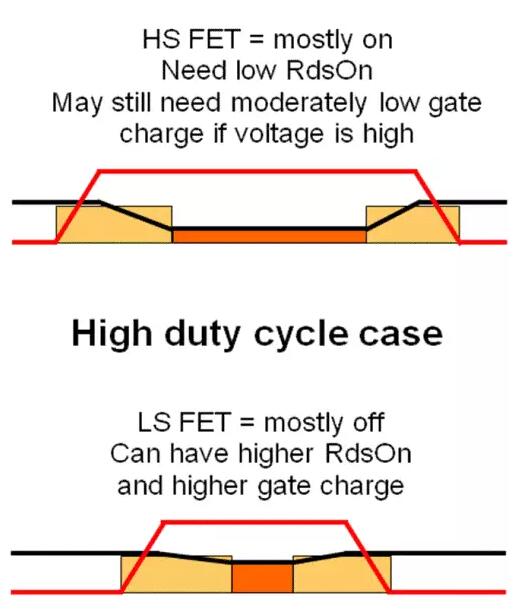
Figure 8— Power Consumption of High-side and Low-side FET with High Duty Cycle Design
Assuming that a point of load (POL) regulator can specify the rated input voltage of an intermediate voltage rail, what is the best solution? Is it high input voltage/low duty cycle or low input voltage/high duty cycle? Use different input voltages to modulate the duty cycle, and check the power consumption of FET.
In fig. 9, the response curve of the high-side FET shows that when the duty cycle increases from 25% to 40%, the AC loss decreases obviously, but the DC loss increases linearly. Therefore, the duty cycle of about 35% should be the ideal value for selecting capacitor and on-resistance balance FET. The lowest AC loss and the highest DC loss can be obtained by continuously decreasing the input voltage and increasing the duty cycle. In this regard, we can use a FET with low on-resistance and choose a high gate charge as a compromise. As shown in Figure 10 of the low-side FET, the controller duty cycle linearly decreases from DC loss when the controller duty cycle is low (the on-time of the low-side FET is shorter), and the loss is the smallest when the controller duty cycle is high. The AC loss of the whole circuit board is very low, so FET with low on-resistance should be selected in any case.
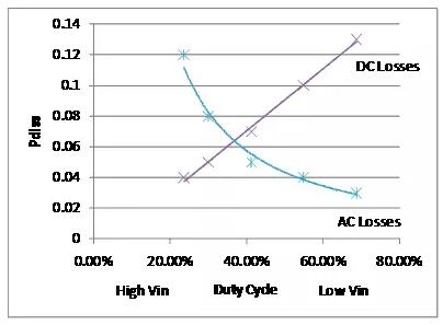
Figure 9-Loss of High Side FET vs. Duty Cycle
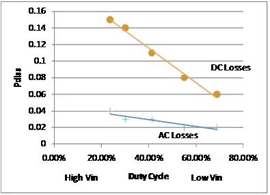
Figure 10— Relationship between Low-side FET Loss and Controller Duty Cycle.
Please note that the duty cycle of the low-side FET is 1- controller duty cycle, so the on-time of the low-side FET decreases with the increase of controller duty cycle.
Figure 11 shows the change of total efficiency when we combine high-side and low-side losses together. We can see that in this case, the combined FET has the lowest loss and the highest efficiency when the duty cycle is high. The efficiency increased from 94.5% to 96.5%. Unfortunately, in order to obtain a low input voltage, we have to reduce the voltage of the intermediate voltage rail power supply and increase its duty cycle, because it is powered by a fixed input power supply. Therefore, this may cancel some or all of the gains obtained at POL. Another method is to directly go from the input power supply to the POL regulator without using the middle rail, in order to reduce the number of regulators. At this time, the duty cycle is low, so we must carefully select the FET.
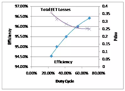
Figure 11— Total Loss vs. Efficiency and Duty Cycle
In the power supply system with multiple output voltage and current requirements, the situation will be more complicated. Compare the efficiency, cost and volume of different duty cycles of POL regulators. Fig. 12 shows a system with an input voltage of 28V, eight loads and four different voltages ranging from 3.3V to 1.25V There are three comparison methods:
1) there is no intermediate rail, and the 28V voltage is directly supplied by the input power supply to realize the low duty cycle of the POL regulator;
2) 12V middle rail is used, and POL regulator has medium duty cycle;
3) Use 5V middle rail, high duty cycle of POL regulator. Figure 13 and Table 1 show the comparison results. In this case, the architecture without middle rail power supply achieves the lowest cost, the architecture with 12V middle rail voltage achieves the highest efficiency, and the architecture with 5V middle rail voltage achieves the smallest volume.
Therefore, we can see that, for this large-scale system, there is no obvious trend of these parameters in the case of single POL power supply. This is because, when multiple regulators are used, except the middle rail regulator itself, each regulator has its own different load current and voltage requirements, which may conflict with each other. The best way to study this situation is to use tools such as WEBENCH Power Designer to evaluate different options.
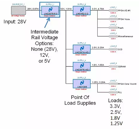
Figure 12— Power supply system showing input, middle rail, point of load (POL) power supply and load.
Different choices of rail voltage are 28V (directly using the input power supply), 12V and 5V. This will result in different duty cycles of POL regulators.
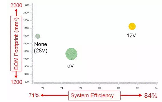
Fig. 13 is a power supply design graph, which shows the influence of the middle rail voltage on the efficiency, volume and cost of the power supply system.
Disclaimer: This article is reproduced from "Power R&D Elite Circle". This article only represents the author's personal views, and does not represent the views of Sacco Micro and the industry. It is only for reprinting and sharing to support the protection of intellectual property rights. Please indicate the original source and author when reprinting. If there is any infringement, please contact us to delete it.。


Site Map | 萨科微 | 金航标 | Slkor | Kinghelm
RU | FR | DE | IT | ES | PT | JA | KO | AR | TR | TH | MS | VI | MG | FA | ZH-TW | HR | BG | SD| GD | SN | SM | PS | LB | KY | KU | HAW | CO | AM | UZ | TG | SU | ST | ML | KK | NY | ZU | YO | TE | TA | SO| PA| NE | MN | MI | LA | LO | KM | KN
| JW | IG | HMN | HA | EO | CEB | BS | BN | UR | HT | KA | EU | AZ | HY | YI |MK | IS | BE | CY | GA | SW | SV | AF | FA | TR | TH | MT | HU | GL | ET | NL | DA | CS | FI | EL | HI | NO | PL | RO | CA | TL | IW | LV | ID | LT | SR | SQ | SL | UK
Copyright ©2015-2025 Shenzhen Slkor Micro Semicon Co., Ltd
