Power devices appeared in the middle of 20th century. After nearly 30 years of development, the combination of MOS and BJT technology gave birth to IGBT technology. After continuous updating, IGBT has been widely used in vehicles, welding, aerospace, and other fields. This paper introduces the structure and working principle of IGBT, and expounds its application in the field of electric vehicles, which is helpful for practitioners to fully understand the principle of IGBT and its technical development in the field of electric vehicles.With the aggravation of global warming and environmental deterioration, in order to alleviate the pressure of energy conservation and emission reduction, China has put forward a high goal. In order to achieve the goal of energy saving and emission reduction, China vigorously supports the development of new energy vehicles. The core energy conversion unit traction inverter of electric vehicle powertrain can convert the DC output from battery into three-phase AC. The frequent start-stop of the vehicle causes the power semiconductor devices in the inverter to bear various impact forces. The power density of inverter is closely related to the power output of electric vehicle. The power semiconductor devices of automotive power modules mainly include silicon carbide-based power metal oxide semiconductor field effect transistors and insulated gate bipolar transistor (IGBT).
IGBT belongs to compound fully controlled voltage driven power semiconductor device, which is composed of bipolar transistor and insulated gate field effect transistor, and has the advantages of high input impedance and low conduction voltage drop. The saturation voltage of giant transistor is low, the current density is high, but the working current is high. Metal half-effect transistor has low working power and fast switching speed, but it has large switching voltage drop and low current-carrying density. IGBT has low power consumption after being turned on, which can be regarded as a conductor, and high resistance when being turned off, which can be regarded as an open circuit. It has three characteristics of high voltage, high current and high speed, low working power and low saturation voltage, and is suitable for converter systems with DC voltage of 600 V or above. Because electric vehicles have high requirements for the voltage resistance, high temperature resistance, heat dissipation and stability of power devices, IGBT has better comprehensive performance than MOSFET transistors. Therefore, IGBT has become the mainstream power device in the inverter of electric vehicles at present, and has great development potential. The IGBT has a grid G, a collector C and an emitter E, and is a three-terminal device. The IGBT has two layers of P+ implantation regions, which form a larger PN junction J1. When the IGBT is connected to the circuit, some carriers are emitted from the injection region P+ to the base region N, which can adjust the conductivity of the drift region. Therefore, the IGBT has a strong current capacity. The buffer region is an N+ layer between the P+ implant region and the N- drift region. Whether there is IGBT in the buffer or not shows different characteristics. IGBT with N+ buffer is called asymmetric IGBT (also called punch-through IGBT), which has the advantages of small forward voltage drop, short dog turn-off time and small tail current when turning off, but its reverse blocking ability is relatively weak. IGBT without N- buffer is called symmetrical IGBT (also called non-punch-through IGBT), which has strong blocking ability in forward and reverse directions, and its other characteristics are worse than those of punch-through IGBT.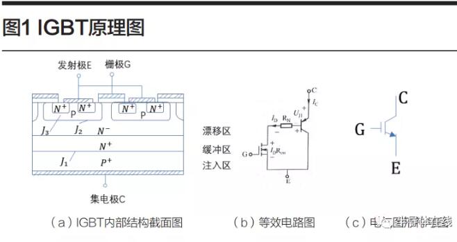
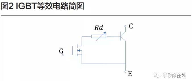
IGBT driving circuit The
IGBT driving circuit is a Darlington structure composed of GTR and
MOSFET, which is turned on and off by controlling the positive and negative voltage of the gate. When the gate voltage is positive, the Darlington transistor composed of GTR and
MOSFET is in a conducting state; When the gate voltage is negative, the Darlington transistor composed of GTR and
MOSFET is in an off state, that is, it does not work. The equivalent circuit diagram of
IGBT drive circuit is shown in Figure 2. This circuit can amplify the pulse output power of single chip microcomputer to indirectly drive
IGBT power devices to work. The volt-ampere characteristic curve is similar to that of
IGBT bipolar giant transistor. When the control voltage UGE increases, the characteristic curve moves upward. Changing the level of UGE can control the state of
IGBT (off-state, saturation state), so it is often used in the switching of power supply.
The working principle of IGBT IGBT can be regarded as a PNP transistor (driven by
MOSFET). Compared with the common PNP transistor, its base region is thicker. The equivalent circuit is shown in Figure 1(b). In the figure, RN is the modulation resistor in the base region of PNP transistor, and
MOSFET is an N-channel field effect transistor. The
IGBT with this structure is called N-channel I
IGBT, and its symbol is N-
IGBT. Similarly, there are P-channel
IGBT, namely P-
IGBT. The electrical graphic symbol of
IGBT is shown in fig. 1(c).
IGBT is a field control device, and its turn-on and turn-off are determined by the voltage UCE between the gate and the emitter. If the turn-on voltage UCE(th) is less than the gate-emitter voltage UCE and the gate voltage is positive, the PNP transistor receives the current in the internal channel of the
MOSFET, and the
IGBT turns on. At this time, the carriers entering the N- region from the P+ region modulate the conductivity of the N- region, and the resistance RN(N- region) will gradually decrease, and the
IGBT will get a smaller on-state voltage drop. If the gate-emitter voltage UCE is equal to zero or the reverse voltage, no channel will be formed in the
MOSFET, no carrier will enter the N- region from the P+ region to modulate the conductivity of the N- region, and there will be no base current in the transistor, so the
IGBT will turn off when it does not work. The driving principle of
IGBT is as follows. When UCE is negative: J3 junction is in reverse bias state and the device is in reverse blocking state. When UCE is positive:UC< UTH,The channel cannot be formed, and the device is in a forward blocking state;UG>UTH,Under the insulated gate, an N channel is formed, and due to the interaction of carriers, conductance modulation is generated in the N- region, which makes the device conduct forward.
1. breakover The difference between the structure of silicon wafer and power MOSFET is that IGBT has more P+ substrate and an N+ buffer layer than power MOSFET (IGBT has no NPT- non-punch-through structure), and a J1 junction is established between P_ region and N+ region of the tube body by using the substrate. If the positive gate bias inverts the P base region under the gate, an N channel will be formed inside the IGBT. At this time, an electron flow and a current will be formed in the channel. When the voltage of the formed electron current is within the range of 0.7 V, J1 established in P_ region and N+ region is in forward bias, and some holes enter into N- region, which will change the resistivity between N- region and N+ region. This adjustment method reduces the energy consumption of IGBT conduction and drives the second charge flow. Two different current topologies, one MOSFET electron current and one hole current (bipolar), temporarily appear in the semiconductor. 2. Conduction voltage drop The conductance modulation effect can reduce the value of resistance RN and the on-state voltage. The so-called on-state voltage drop refers to the tube voltage drop UDS when the IGBT enters the on state, and this voltage decreases with the UCS rising. 3. shutoff When a negative bias voltage is applied to the gate or the gate voltage is lower than the threshold value, no channel will be formed and no holes will enter the N- region. In all cases, if the MOSFET current drops too fast in the switching stage, the collector current will decrease. At this time, after the commutation starts, a few carriers still remain in the N region. The density of charge at turn-off will directly affect the reduction of residual current value. The charge density is related to the number and topology of impurities, the thickness and temperature of layers, etc. Therefore, reducing the residual current value (wake) is affected by many factors and uncertain. The collector current is affected by the decay of some residual carriers in the N region, and the characteristic wake waveform appears. Characteristic collector wake will cause problems such as high power consumption and disordered conduction. This kind of problem will be more prominent in the equipment of freewheeling diode. Because the residual current is closely related to the recombination of minority carriers, the current value of the residual current should have an important relationship with Tc, IC, UCE and hole mobility of the chip.4. Reverse blocking If the collector gets the reverse voltage, the J junction of P_ region and N+ region will be affected by the reverse bias voltage. At the same time, the blocking ability will be lost because the thickness of the layer decreases too much, and the depletion layer will extend to the N- region. In addition, if the region size increases beyond a certain value, the voltage drop will increase continuously. 5. Forward blocking If the collector terminal gets positive voltage and the gate and emitter are shorted, the J junction between P_ region and N+ region is controlled by reverse voltage. 6. latch PNPN thyristor is parasitic between the collector and emitter of ICBT. The thyristor conduction phenomenon is called IGBT latch-up. Under certain conditions, the PNPN thyristor will conduct, the current between the collector and emitter will increase, and the ability to control the equivalent MOSFET will decrease, which often leads to the breakdown of the device. And the development history of IGBT chips in electric vehicles. Looking back at the development of power devices in the past decades, in 1960s, bipolar devices had small on-state resistance, complicated current control and control circuit, and high power consumption. With the development of industry, the requirements of simplifying the driving circuit, reducing the manufacturing cost, switching power consumption and on-state voltage drop are put forward to the academic circles. In 1990s, IGBT was manufactured under the background of the research of MOS and BJT integration technology. The emergence of IGBT is not for the service of electric vehicles. However, with the deterioration of the global environment, electric vehicles have developed, and IGBT has gradually begun to be applied in the fields of automobiles, transportation, etc. With the common development of electric vehicles and IGBT, IGBT chips have become an indispensable part of electric vehicles. The development process of IGBT chips for electric vehicles is shown in Figure 3. The first generation: the prototype of IGBT, which needs to improve the withstand voltage by increasing N-drift, has high off-power consumption and on-resistance. Due to the above factors, the first generation IGBT stopped in the laboratory and was not widely used. The second generation: PT-IGBT. The depletion layer fails to penetrate the N+ buffer layer, and the electric field in the base region is strengthened in a trapezoidal distribution. The power consumption is reduced by reducing the chip thickness. Siemens was the representative company that produced IGBT devices at that time. At the end of the 20th century, BSM150GB120DN1(DN1 stands for the first generation product) produced by Siemens has a good performance at 600V voltage, but when the voltage rises to 1200 V, the epitaxial thickness becomes larger, the cost is relatively high, and the reliability decreases (the uniformity of doping concentration and thickness is poor). The third generation: NPT-IGBT. Ion implantation technology replaces epitaxial technology to generate P+ collector (transparent collector technology), which can control junction depth well and ensure the lowest emission efficiency as possible. Turn-off loss is realized by speeding up carrier extraction. The original carrier lifetime of the base region is not affected basically, and the influence on the steady-state power consumption is almost negligible. At this time, the IGBT has the characteristics of positive temperature coefficient, and performs well between the steady-state loss and the turn-off loss. At this time, the representative company of IGBT is still Siemens, which adopts zone melting method to replace the extended batch products. The fourth generation: Trench-IGBT. The fourth generation has a great improvement compared with the past. This time, the trench structure is used, and the channel moves from the previous surface to the vertical surface, which enhances the PIN effect in the base region, increases the concentration of carriers near the gate, improves the conductance modulation effect to some extent, reduces the on-resistance and eliminates the JFET effect. The gate density can be increased as required. In addition, the fourth generation continues to inherit the collector P+Implicit technology of the third generation, and introduces PT technology as the field stop layer, which improves the withstand voltage. Infineon replaced Siemens as the leading enterprise, and its thinning technology was the first in the world at that time. At 1200 V, its thickness could be between 120 and 140 um, and at 600V, it could be below 70 um. The fifth and sixth generation: the fifth generation FS-IGBT and the sixth generation FS-Trench are the recombination of various technical measures based on the previous four technologies. The fifth generation IGBT is the combination of the fourth generation product "transparent collector technology" and "electric field stop technology". The difference between the sixth generation product and the fifth generation product is that the trench gate structure is improved. In the field of electric vehicles, IGBT is used as the mainstream device of new power semiconductor devices, which is widely used in rail transit, new energy vehicles and other fields. At present, with the accelerated pace of life, the market puts forward higher requirements for the power, safety and price of new energy vehicles, and the current density, power loss and stability of IGBT play an important role.

The development of electric vehicles is closely related to the development of IGBT modules, and electric vehicles, charging piles and related equipment are all inseparable from the support of IGBT technology. In the production cost of electric vehicles, IGBT modules account for more than 10%, accounting for nearly 1/5 of the production cost of charging piles. In the field of electric vehicles, IGBT is mainly used in the following aspects: 1. Control system of electric vehicles IGBT technology is used to control high-power DC/AC inverter and then control the operation of motor. Converter is the core component of traction in AC drive system, and IGBT is the key component of traction converter. 2. The vehicle air conditioning control system uses IGBT and FRD with low current to control low-power DC/AC inverter. 3. IGBT module of charging pile is used as switching element in intelligent charging pile. tag
IGBT has good performance in high current density, low loss optimization technology, high temperature and high voltage technology and intelligent integration technology. It has been widely used in power modules of new energy vehicles and has a good prospect. However, to realize the large-scale application of IGBT chip optimization technology for electric vehicles, it is necessary to further optimize the fineness, high temperature and high pressure resistance and multi-functional integration technology of trench gate.
Disclaimer: This article is reproduced from "Semiconductor Online". This article only represents the author's personal views, and does not represent the views of Sacco Micro and the industry. It is only for reprinting and sharing to support the protection of intellectual property rights. Please indicate the original source and author when reprinting. If there is any infringement, please contact us to delete it.
Company Tel: +86-0755-83044319
Fax/fax:+86-0755-83975897
Email: 1615456225@qq.com
QQ: 332496225 Manager Qiu
Address: Room 809, Block C, Zhantao Technology Building, No.1079 Minzhi Avenue, Longhua New District, Shenzhen


