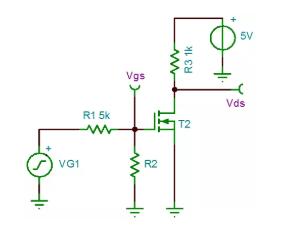
It is an NMOS switching circuit. The step signal VG1 sets the DC level 2V, the square wave (amplitude 2V, frequency 50Hz) and the turn-on voltage 2V of T2, so the MOS transistor T2 will switch between the on and off states with a period T = 20 ms.
 First, simulate the waveforms of Vgs and Vds, and you will see that there is a small platform when Vgs=2V. Some people will wonder why Vgs has a small platform when it rises?
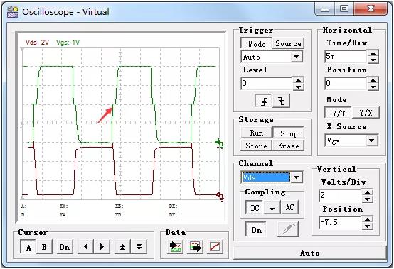
Mosvgs small platform With this question in mind, we tried to change the resistance R1 from 5K to 1K, and simulated again, and found that this platform became very small, almost gone. Why?
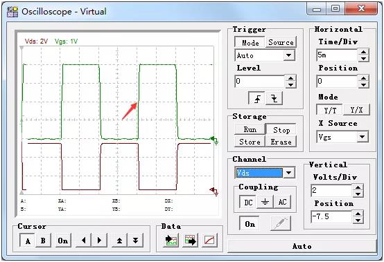 The MOS Vgs small platform is improved.
To understand this phenomenon, we need the support of theoretical knowledge. 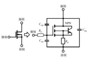 Equivalent model of MOS tube
We usually see the figure of MOS tube on the left, and the figure on the right is called the equivalent model of MOS tube. Among them, Cgs is called GS parasitic capacitance, Cgd is called GD parasitic capacitance, input capacitance Ciss=Cgs+Cgd, output capacitance Coss=Cgd+Cds, reverse transmission capacitance Crss=Cgd, also called Miller capacitance.If you don't know the concept of input and output capacitance of MOS tube, please click: to show you the parameters of MOS tube "thermal resistance, input and output capacitance and switching time"The chief culprit of Miller effect is Miller capacitance. Miller effect refers to the effect that the distributed capacitance Cgd between its input and output is amplified under the action of inverse amplification, which makes the equivalent input capacitance value enlarged. Miller effect will form Miller platform.
Equivalent model of MOS tube
We usually see the figure of MOS tube on the left, and the figure on the right is called the equivalent model of MOS tube. Among them, Cgs is called GS parasitic capacitance, Cgd is called GD parasitic capacitance, input capacitance Ciss=Cgs+Cgd, output capacitance Coss=Cgd+Cds, reverse transmission capacitance Crss=Cgd, also called Miller capacitance.If you don't know the concept of input and output capacitance of MOS tube, please click: to show you the parameters of MOS tube "thermal resistance, input and output capacitance and switching time"The chief culprit of Miller effect is Miller capacitance. Miller effect refers to the effect that the distributed capacitance Cgd between its input and output is amplified under the action of inverse amplification, which makes the equivalent input capacitance value enlarged. Miller effect will form Miller platform.
The first thing we need to know is: because the manufacturing process of MOS tube will definitely produce Cgd, that is, Miller capacitor must exist, so Miller effect is inevitable. What are the disadvantages of Miller effect? The turning-on of MOS transistor is a process from scratch. The longer the overlapping time of D pole and S pole of MOS transistor, the greater the conduction loss of MOS transistor. Because of the Miller capacitor and the Miller platform, the turn-on time of the MOS tube becomes longer, and the conduction loss of the MOS tube is bound to increase. When we reduced the resistance R1 of G pole in simulation, we found that the Miller platform was improved? We should all know why. The turning-on of MOS transistor can be seen as the charging process of parasitic capacitance Cgs by input voltage through gate resistance R1. The smaller R1 is, the faster Cgs charges and the faster MOS transistor turns on, which is the reason for reducing gate resistance and improving Miller platform. So what happened on Miller Platform?
For NMOS transistor, before the MOS transistor is turned on, the D-pole voltage is greater than the G-pole voltage. With the increase of the input voltage, Vgs increases, and the charge stored in Cgd needs to be neutralized with the input voltage at the same time, because the G-pole voltage is greater than the D-pole voltage when the MOS transistor is fully turned on.
Therefore, on the Miller platform, it is the process of Cgd charging, and at this time, the change of Vgs is very small. When Cgd and Cgs are at the same level, Vgs begins to continue to rise.
Let's analyze the Miller effect in the following picture on the right,What is the situation of this circuit diagram?
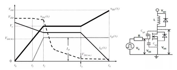 The D-pole load of MOS transistor is an inductor plus a freewheeling diode, which works in the same mode as DC-DC BUCK. When the MOS transistor is turned on, VDD charges the inductor L. Because the MOS transistor has a very short turn-on time, the inductor can be approximated as a constant current source. When the MOS transistor is turned off, the freewheeling diode provides a discharge path for the inductor L to form a freewheeling current.The opening of MOS tube can be divided into four stages. t0~t1阶段 From t0, the G pole charges the capacitor Cgs. When Vgs rises from 0V to Vgs(th), the MOS transistors are all in the off state, Vds remains unchanged, and Id is zero. t1~t2阶段 After t1, Vgs is greater than the turn-on voltage Vgs(th) of the MOS transistor, and the MOS transistor starts to conduct, and the Id current rises. The equivalent circuit diagram at this time is shown below. When the IDS current does not reach the inductor current, a part of the current will flow through the diode, and the diode DF is still in a conducting state, and both ends of the diode are in a clamping state. At this time, the Vds voltage is almost unchanged, with only a small drop (the influence of stray inductance).
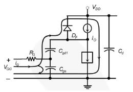
T2~t3 stage With the increase of Vgs voltage, when the IDS current is the same as the inductor current, the D-pole voltage of MOS tube is no longer clamped by the diode DF, and DF is in the reverse cut-off state, so Vds begins to drop. At this time, the driving current of G-pole is transferred to Cgd for charging, and the Miller platform appears in Vgs, the Vgs voltage remains unchanged, and Vds gradually drops to the on-voltage drop VF.
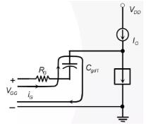
From T3 to T4, when the Miller capacitor Cgd is fully charged, the Vgs voltage continues to rise until the MOS transistor is completely turned on.
Combined with the output curve of MOS tube, summarize the conduction process of MOS tube.
From t0 to t1, the MOS tube is in the cut-off zone; After t1, Vgs exceeds the turn-on voltage of MOS transistor. With the increase of Vgs, ID increases. When ID rises to the same level as the inductor current, the freewheeling diode turns off in reverse. During t2~t3, Vgs enters the Miller plateau. At this time, the voltage of D pole is no longer clamped by the freewheeling diode, and the pinch-off region of MOS becomes smaller. After t3, Vgs continues to rise and Vds gradually decreases until the MOS transistor is completely turned on.
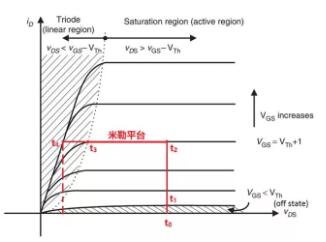
Output curve of MOS tube
Disclaimer: This article is reproduced from "The Lion Attacking the City on Line 8". This article only represents the author's personal views, and does not represent the views of Sacco Micro and the industry. It is only for reprinting and sharing to support the protection of intellectual property rights. Please indicate the original source and author when reprinting. If there is any infringement, please contact us to delete it.
Company Tel: +86-0755-83044319
Fax/fax:+86-0755-83975897
Email: 1615456225@qq.com
QQ: 332496225 Manager Qiu
Address: Room 809, Block C, Zhantao Technology Building, No.1079 Minzhi Avenue, Longhua New District, Shenzhen


