Service hotline
+86 0755-83044319

release time:2022-03-17Author source:SlkorBrowse:13401
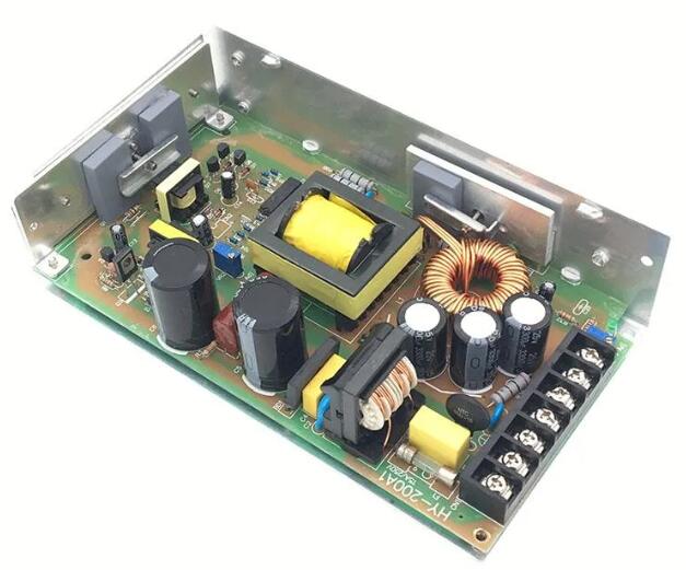
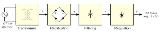
Figure 1: Standard linear power supply design diagram
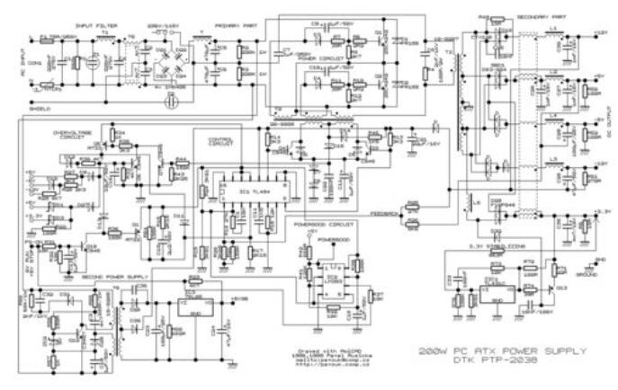
Figure 2: Waveform of linear power supply
Although linear power supply is very suitable for supplying power to low-power devices, such as cordless phones, PlayStation/Wii/Xbox and other game consoles, for high-power devices, linear power supply will be inadequate.
For linear power supply, the size of its internal capacitance and transformer is inversely proportional to the frequency of AC mains: that is to say, if the frequency of input mains is lower, the larger capacitance and transformer are needed for linear power supply, and vice versa. At present, AC mains with a frequency of 60Hz (50Hz in some countries) is always used, which is a relatively low frequency, so the size of its transformer and capacitor is often relatively large. In addition, the bigger the surge of AC mains, the bigger the transformer of linear power supply.
Therefore, for the field of personal PC, manufacturing a linear power supply will be a crazy move, because its volume will be very large and its weight will be very heavy. Therefore, personal PC users are not suitable for sharing linear power supply.
● How much do you know about switching power supply?
Switching power supply can solve this problem well through high-frequency switching mode. For high-frequency switching power supply, the AC input voltage can be boosted before entering the transformer (usually 50-60 KHz before boosting).With the increase of input voltage, the size of components such as transformers and capacitors doesn't have to be as big as linear power supply.
This high-frequency switching power supply is just what our personal PC and equipment like VCR need.It should be noted that what we often call "switching power supply" is actually the abbreviation of "high-frequency switching power supply", which has nothing to do with the turn-off and turn-on of the power supply itself.In fact, the power supply of the end user's PC adopts a more optimized scheme: closed loop system-the circuit responsible for controlling the switching tube, obtaining the feedback signal from the output of the power supply, and then increasing or decreasing the frequency of the voltage in a certain period according to the power consumption of the PC so as to adapt to the transformer of the power supply (this method is called PWM, Pulse Width Modulation, pulse width modulation).Therefore, the switching power supply can be self-adjusted according to the power consumption of the connected power-consuming equipment, so that the transformer and other components can take away less energy and reduce the calorific value.
On the other hand, the design concept of linear power supply is that power is paramount, even if the load circuit does not require a large current. The consequence of this is that all components work at full load even when not necessary, resulting in much higher heat.
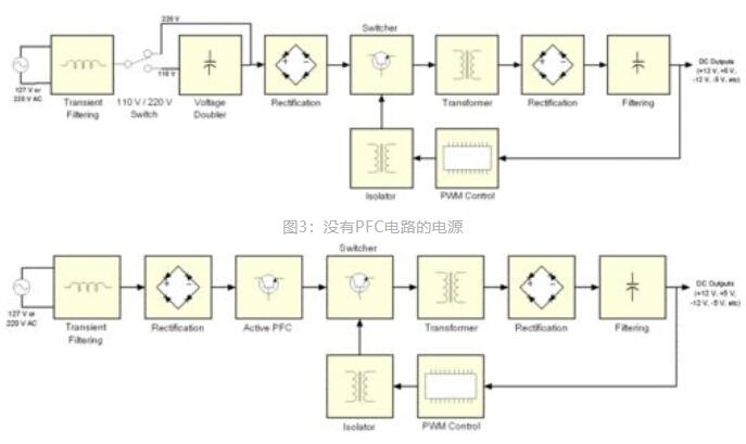
Figure 4: Power supply with PFC circuit
By comparing Figure 3 with Figure 4, we can see the difference between them: one has an active PFC circuit and the other does not. The former has no 110/220 V converter and no voltage doubling circuit. The following will focus on the explanation of active PFC power supply.In order for readers to better understand the working principle of the power supply, the above is a very basic diagram, which does not include other additional circuits, such as short-circuit protection, standby circuit and PG signal generator. Of course, if you want to know a more detailed diagram, please see Figure 5. It doesn't matter if you can't understand it, because this picture is originally for those professional power designers.
Figure 5: Typical design diagram of low-end ATX power supply (the picture may not be clear, so I suggest you drag it out for a look)
You may ask, why is there no voltage rectification circuit in the design diagram of Figure 5? In fact, the PWM circuit has already shouldered the work of voltage rectification. The input voltage will be corrected again before passing through the switch tube, and the voltage entering the transformer has become a square wave. Therefore, the waveform of the transformer output is also a square wave, not a sine wave. At this time, the waveform is square, so the voltage can be easily converted into DC voltage by the transformer.
That is to say, after the voltage is recalibrated by the transformer, the output voltage has become DC DC voltage. That's why switching power supply is often called DC-DC converter.The loop of the PWM control circuit is responsible for all the required regulating functions. If the output voltage is wrong, the PWM control circuit will change the control signal of the duty cycle to adapt to the transformer, and finally correct the output voltage. This often happens when PC power consumption increases, and the output voltage tends to decrease, or when PC power consumption decreases, the output voltage tends to increase.When looking at the next page, it is necessary for us to know the following information:
★ All circuits and modules before the transformer are called "primary side", and all circuits and modules after the transformer are called "secondary side";
★ The power supply designed with active PFC does not have a 110 V/ 220 V converter and a voltage doubler;★ For the power supply without PFC circuit, if 110 V/220 V is set to 110 V, before the current enters the rectifier bridge, the power supply itself will use the voltage doubler to raise 110 V to about 220 V;
★ The switch tube on the PC power supply consists of a pair of power MOSFET tubes, of course, there are other combinations, which we will explain in detail later;
★ The required waveform of the transformer is square wave, so the voltage waveform after passing through the transformer is square wave, not sine wave;
★PWM control current is often an integrated circuit, usually isolated from the primary side by a small transformer, but sometimes it may be isolated from the primary side by a coupling chip (a small IC chip with LED and phototransistor);
★PWM control circuit controls the closing of the switch tube of the power supply according to the output load of the power supply. If the output voltage is too high or too low, the PWM control circuit will change the voltage waveform to adapt to the switching tube, so as to achieve the purpose of correcting the positive output voltage;
On the next page, we will study each module and circuit of the power supply through pictures, and visually tell you where to find them in the power supply through physical pictures.
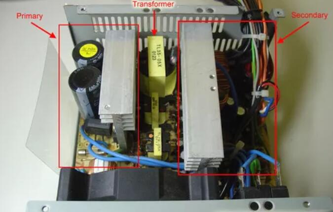
Distinguish primary side from secondary side.
Above, we have roughly introduced each module inside a power supply from a macro perspective. Let's refine it and turn the topic to the components of each module of power supply ...
04
Analysis of transient filter circuit
After being connected to the PC switching power supply, the commercial power first enters the Transient Filtering circuit, which is commonly referred to as EMI circuit. The following figure describes the circuit diagram of the "recommended" transient filter circuit of a PC power supply.
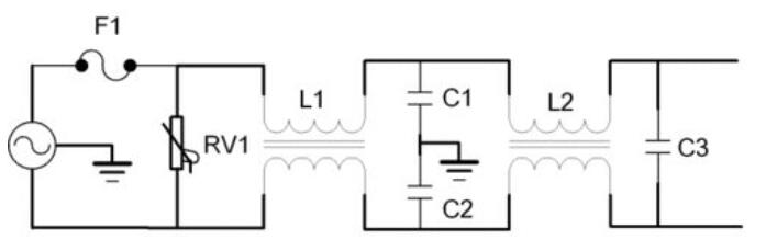
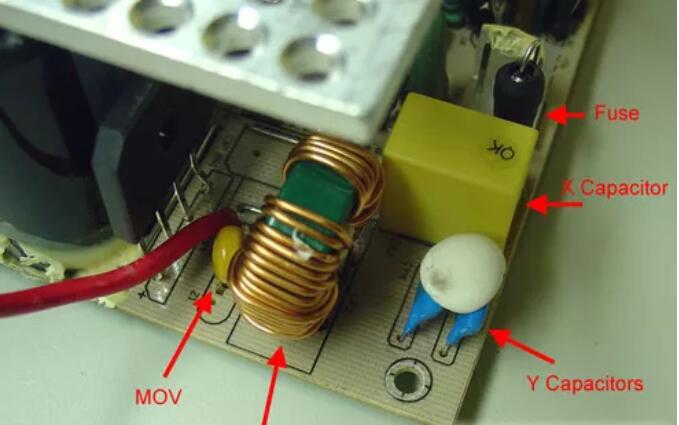
Circuit diagram of transient filter circuit
Why should we emphasize that it is "recommended"? Because many power supplies on the market, especially low-end power supplies, often omit some components in Figure 8. So you can judge the quality of your power supply by checking whether the EMI circuit has shrunk.
The main component of EMI circuit is MOV (Metal Oxide Varistor), or varistor (RV1 in Figure 8), which is responsible for suppressing the peak in the transient of commercial power. The MOV element is also used in surge suppressors. However, many low-end power supplies often cut off important MOV components in order to save costs. For the power supply equipped with MOV elements, it is not important whether there is a surge suppressor or not, because the power supply already has the function of suppressing surge.
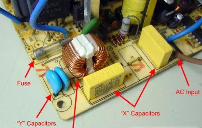
L1 and L2 in fig. 8 are ferrite coils; C1 and C2 are disk capacitors, usually blue, and these capacitors are usually called "Y" capacitors; C3 is a metallized polyester capacitor, usually with a capacity of 100nF, 470nF or 680nF, also called "X" capacitor; Some power supplies are equipped with two X capacitors, which are connected in parallel with the mains, as shown in Figure 8 RV1.
X capacitor can be any capacitor connected in parallel with the mains; Y capacitors are usually paired in pairs, which need to be connected in series between fire and zero and the midpoint of the two capacitors should be grounded through the chassis. That is to say, they are connected in parallel with the mains.
The transient filter circuit can not only filter the commercial power, but also prevent the noise generated by the switching tube from interfering with other electronic devices on the same commercial power.
Let's take a look at some practical examples. As shown in Figure 9, can you see some strange things? This power supply has no transient filter circuit! This is a cheap "cottage" power supply. Please note, look at the mark on the circuit board. The transient filter circuit should have been there, but it was brought to the market by the heartless JS.
This cheap "cottage" power supply has no transient filter circuit.
As shown in Figure 10, this is a low-end power supply with transient filter circuit, but as we can see, the transient filter circuit of this power supply omits the important MOV varistor and only has a ferrite coil; However, this power supply is equipped with an extra X capacitor.
EMI circuit of low-end power supply
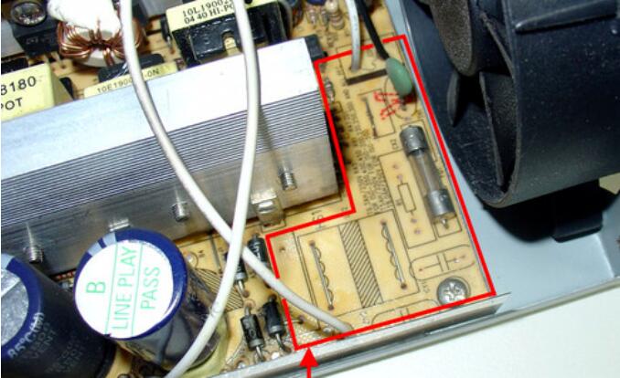
Transient filter circuits are divided into primary EMI and secondary EMI. The primary EMI of many power supplies is often placed on an independent PCB, close to the mains interface, while the secondary EMI is placed on the main PCB of the power supply, as shown in the following figures 11 and 12.Class I EMI is equipped with an X capacitor and a ferrite inductor.
Look at the secondary EMI of this power supply. Here we can see the MOV varistor, although its placement is a bit strange, behind the second ferrite. Overall, it should be said that the EMI circuit of this power supply is very complete.
Complete secondary EMI
It is worth mentioning that the MOV varistor of the above power supply is yellow, but in fact most MOVs are dark blue.
In addition, the transient filter circuit of this power supply is equipped with a fuse (shown as F1 in Figure 8). It should be noted that if you find that the fuse in the fuse tube has been blown, then it is certain that one or some components inside the power supply are defective. It's useless to replace the fuse at this time, and it will probably be burned out again after you turn it on.
05
Voltage doubler and primary rectification circuit
● Voltage doubler and primary rectification circuit
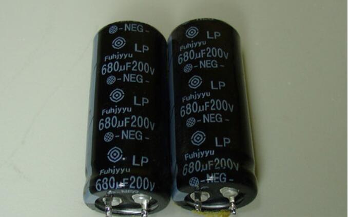
As mentioned above, switching power supply mainly includes active PFC power supply and passive PFC power supply. The latter has no PFC circuit but is equipped with a voltage doubler. The voltage doubler uses two huge electrolytic capacitors, that is to say, if you see two large capacitors inside the power supply, it can basically be judged that this is the voltage doubler of the power supply. As we mentioned earlier, the voltage doubler is only suitable for areas with 127V voltage.
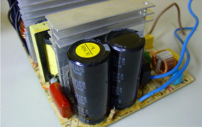
A voltage doubler composed of two huge electrolytic capacitors
Take it down and have a look
The rectifier bridge can be seen on one side of the voltage doubler. The rectifier bridge can be composed of four diodes or a single component, as shown in Figure 15. The rectifier bridge of high-end power supply is usually placed on a special heat sink.
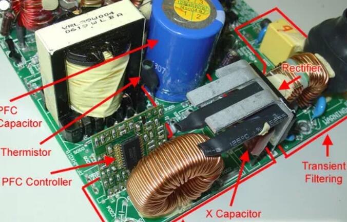
rectifier bridge
In the primary part, there is usually an NTC thermistor, which can change the resistance value according to the change of temperature. NTC thermistor is the abbreviation of Negative Temperature Coefficient. Its function is mainly to re-match the power supply when the temperature is very low or very high, which is similar to the ceramic disk capacitor, usually olive.
06Active PFC circuit
● Active PFC circuitUndoubtedly, this kind of circuit can only be seen in the power supply equipped with active PFC circuit.
Figure 16 illustrates a typical PFC circuit:
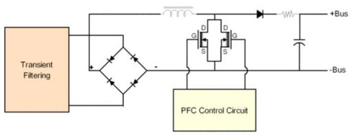
Active PFC circuit diagram
Active PFC circuit usually uses two power MOSFET switches. These switch tubes are usually placed on the heat sink of the primary side. For easy understanding, we have marked each MOSFET switch tube with letters: S stands for Source, D stands for Drain, and G stands for Gate.
PFC diode is a power diode, which usually adopts a similar packaging technology as power transistor. They are similar in length, and are also placed on the heat sink of the primary side, but PFC diode has only two pins.
The inductance in PFC circuit is the largest inductance in power supply; The filter capacitor on the primary side is the largest electrolytic capacitor on the primary side of active PFC power supply. The resistor in fig. 16 is an NTC thermistor, which can change the resistance value with the change of temperature, and has the same function as the NTC thermistor of secondary EMI.Active PFC control circuit is usually based on an IC integrated circuit, and sometimes this integrated circuit is also responsible for controlling the PWM circuit (used to control the closing of the switch tube). This kind of integrated circuit is usually called "PFC/PWM combo".
As usual, look at some examples first. In Figure 17, we can see the components better after removing the heat sink on the primary side. It is the secondary EMI circuit of the transient filter circuit on the left, which has been introduced in detail above; Look at the left side, all of them are components of active PFC circuit.
Since we have removed the heat sink, the PFC transistor and the PFC diode can't be seen in the picture. In addition, if you pay a little attention, you can see that there is an X capacitor (brown element at the bottom of the heat sink of the rectifier bridge) between the rectifier bridge and the active PFC circuit. Usually, the olive thermistor, which looks like a ceramic disk capacitor, is covered with rubber.
Active PFC components
Fig.18 is an element on the primary side heat sink. This power supply is equipped with two MOSFET switches and power diodes of active PFC circuit:
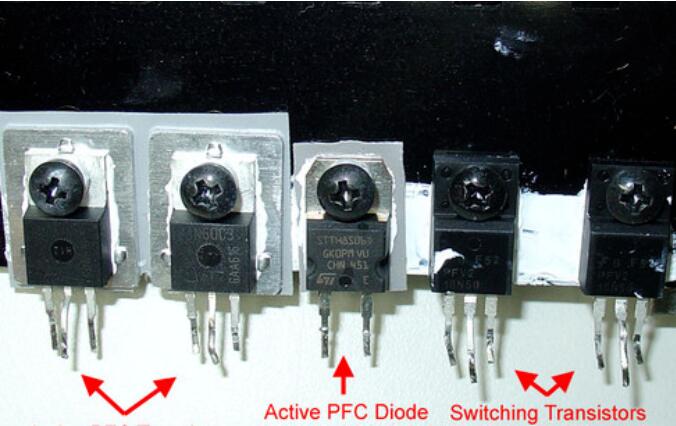
Switch, power diode
Next, we will focus on the switch tube …
07
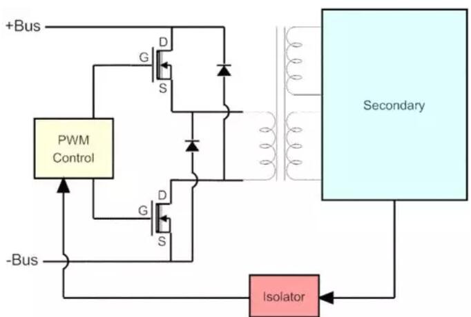
switch tube
● Switch tubeThe switching inverter of the power supply can have many modes. We have summarized the following situations:
| 模式 | 开关管数量 | 二极管数量 | 电容数量 | 变压器针脚 |
| 单端正激 | 1 | 1 | 1 | 4 |
| 双管正激 | 2 | 2 | 0 | 2 |
| 半桥 | 2 | 0 | 2 | 2 |
| 全桥 | 4 | 0 | 0 | 2 |
| 推挽 | 2 | 0 | 0 | 3 |
Of course, we only analyze how many components are needed in a certain mode. In fact, engineers will be restricted by many factors when considering which mode to adopt.
At present, the two most popular modes are the two-transistor forward design and the push-pull design, both of which use two light switches. We have already introduced these light-emitting tubes which are arranged on the primary side heat sink on the previous page, so I won't repeat them here.
Here are the design drawings of these five modes:
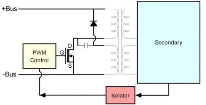
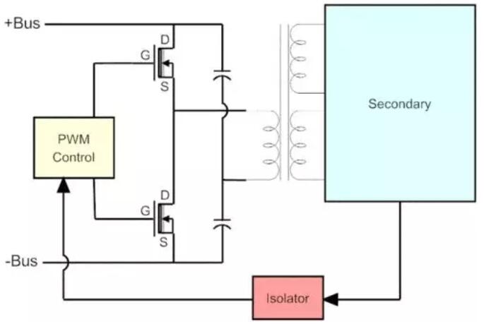
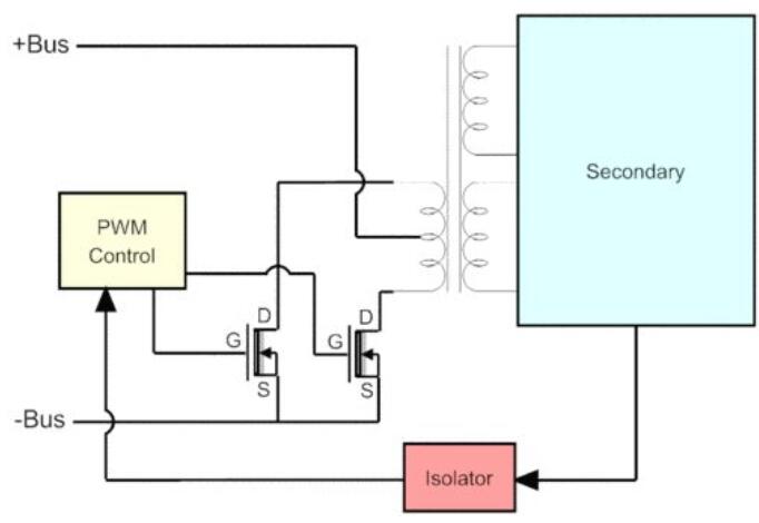
(Single-transistor forward configuration)
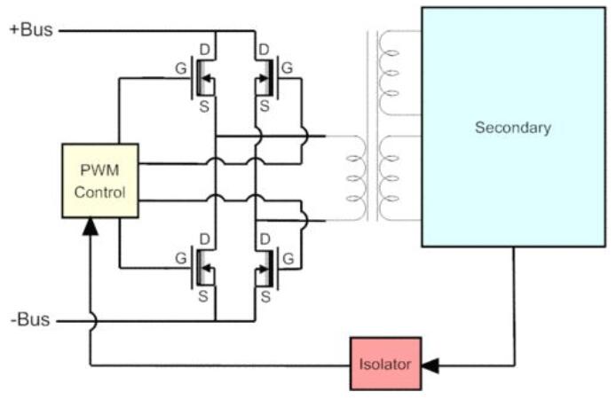
(Two-transistor forward configuration)
(Half bridge configuration)
(Full bridge configuration)
(Push-pull configuration)
8、And a transformer PWM control circuit.
● Transformer and PWM control circuit
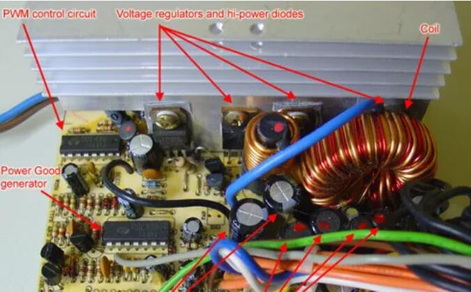
As we mentioned earlier, PC power supply is generally equipped with three transformers: the biggest one is the main transformer marked in previous Figures 3, 4 and 19-23. Its primary side is connected with the switch tube, and its secondary side is connected with the rectifier circuit and filter circuit, which can provide low-voltage DC output (+12V, +5V, +3.3V, -12V, -5V) of the power supply.
The smallest transformer has a load of +5VSB output, which usually becomes a standby transformer, and is always in a "standby state" because this part of the output is always on, even when the PC power is off.The third transformer is an isolator, which connects the PWM control circuit with the switch tube. Not all power supplies will be equipped with this transformer, because some power supplies are often equipped with optocoupler integrated circuits with the same function.
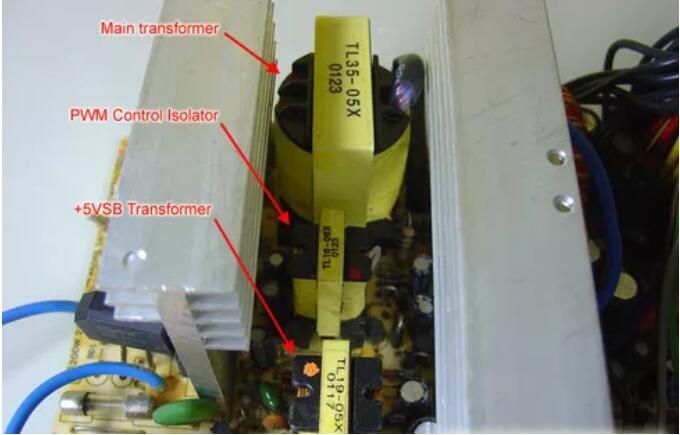
transformer
This power supply uses optocoupler integrated circuit instead of transformer.
The PWM control circuit is based on an integrated circuit. Generally, the power supply without active PFC will adopt TL494 integrated circuit (the compatible DBL494 integrated chip is adopted in Figure 26 below). In the power supply with active PFC circuit, a chip used to replace PWM chip and PFC control circuit is sometimes used. CM6800 chip is a good example, which can integrate all functions of PWM chip and PFC control circuit.
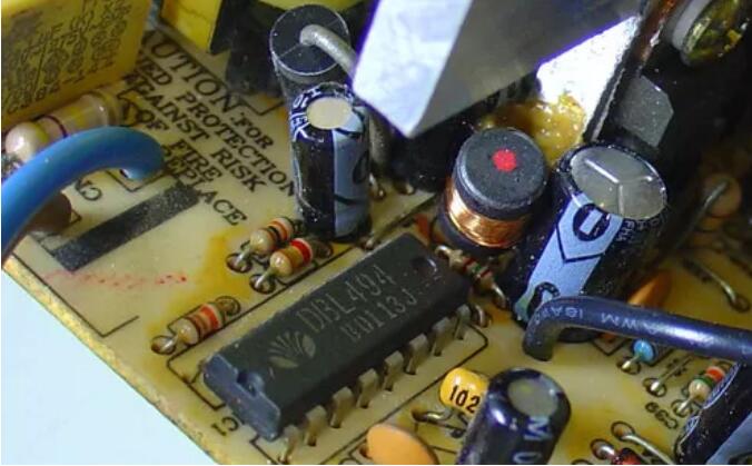
PWM control circuit
08Secondary side (1)
● Secondary side
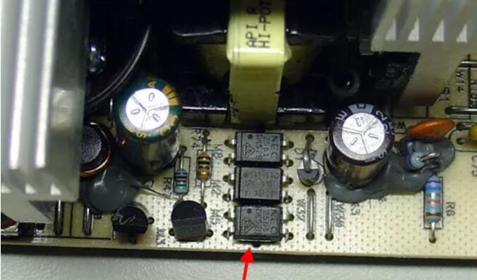
Finally, the secondary side is introduced. At the secondary side, the output of the main transformer will be rectified and filtered, and then the voltage required by PC will be output. Rectification of -5 V and–-12 V can be done only with ordinary diodes, because they don't need high power and large current.
However, the rectification tasks of positive voltages such as +3.3 V, +5 V and +12 V need a high-power Schottky rectifier bridge. This Schottky has three pins, which are similar in appearance to power diodes, but they have two high-power diodes integrated inside. Whether the secondary side rectification can be completed is determined by the power circuit structure. Generally, there may be two kinds of rectification circuit structures, as shown in Figure 27:
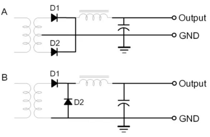
Rectification mode
Mode A will be more used in low-end entry-level power supply. This mode requires three pins from the transformer. Mode B is mostly used in high-end power supply. Generally, this mode only needs to be equipped with two transformers, but the ferrite inductance must be large enough, so this mode costs more, which is the main reason why low-end power supply does not adopt this mode.
In addition, for high-end power supplies, in order to improve the maximum current output capacity, these power supplies often double the maximum current output of the rectifier circuit by connecting two diodes in parallel.
Whether it is a high-end or low-end power supply, its +12 V and +5 V outputs are equipped with complete rectifier circuits and filter circuits, so all power supplies need at least two sets of rectifier circuits as shown in Figure 27.
There are three options to choose from for 3.3V output:
☆ Add a 3.3V voltage regulator in the +5 V output part, which is adopted by many low-end power supplies;
☆ Add a complete rectifier circuit and filter circuit as shown in Figure 27 for the 3.3 V output, but it needs to share a transformer with the 5 V rectifier circuit. This is a common design scheme of high-end power supply.
☆ Adopt a complete and independent 3.3V rectifier circuit and filter circuit. This kind of scheme is very rare, and it can only appear in a few top-level power sources with fever level, such as the Galaxy 1000W of Annette.
Because 3.3V output is usually a fully shared 5V rectifier circuit (common in low-end power supply) or partially shared (common in high-end power supply), it is said that 3.3V output is often limited by 5V output. That's why many power supplies should be named "3.3V and 5V combined output" on the nameplate.Figure 28 below shows the secondary side of a low-end power supply. Here we can see the integrated circuit responsible for generating PG signals. Generally, LM339 integrated circuit is used for low-end power supply.
secondary side
In addition, we can also see some electrolytic capacitors (the size of these capacitors is much smaller than that of voltage doubler or active PFC circuit) and inductors, which are mainly responsible for filtering function.
In order to observe this power supply more clearly, we have removed all flying wires and filter coils on the power supply, as shown in Figure 29. Here we can see some small diodes, which are mainly used for rectification of-12 V and–5 V, and the current passing through them is very small (this power supply only needs 0.5A). The output current of other voltages should be at least 1A, which requires the power diode to be responsible for rectification.
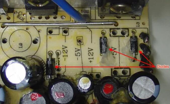
Rectifier diodes for–-12 V and–5 V negative voltage circuits
10. Secondary side (II)
● Secondary side
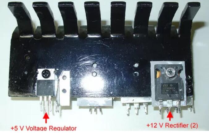
(2)The following figure depicts the components on the secondary side heat sink of low-end power supply:
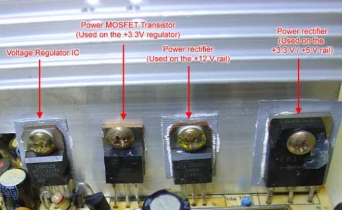
Components on the secondary heat sinkFrom left to right:
☆ IC chip of voltage regulator-although it has three pins and looks very similar to a triode, it is an IC chip. This power supply uses 7805 voltage regulator (5V voltage regulator), which is responsible for the voltage stabilization of +5VSB. As we mentioned before, the +5VSB adopts an independent output circuit, because it still needs to provide +5 V output to the +5VSB even when the PC is powered off. That's why the +5VSB output is also commonly referred to as "standby output". The 805IC can provide a maximum current output of 1A.
☆ Power MOSFET transistor, mainly responsible for 3.3V output. The MOSFET model of this power supply is PHP45N03LT, which can allow the maximum current of 45A to pass through. As we mentioned on the previous page, only the low-end power supply will adopt the 3.3V regulator shared with 5V.
☆ Power Schottky rectifier, which is formed by integrating two diodes. The Schottky model of this power supply is STPR1620CT, and each diode of this power supply can allow a maximum current of 8A (16A in total). This kind of power Schottky rectifier is usually used for 12V output.
☆ Another power Schottky rectifier. The model of this power supply is E83-004, and the maximum allowable current is 60A. This power rectifier is often used for +5 V and+3.3 V outputs. Because the +5 V and+3.3 V outputs use the same rectifier, the sum of them cannot exceed the current limit of the rectifier. This is what we often call the concept of joint output. In other words, the 3.3V output comes from the 5V output. Unlike other outputs, the transformer has no 3.3V output. This design is often used for low-end power supply. Generally, independent +3.3 V and +5 V outputs are used in the high-end power supply.
Let's take a look at the main components of the secondary side of the high-end power supply:
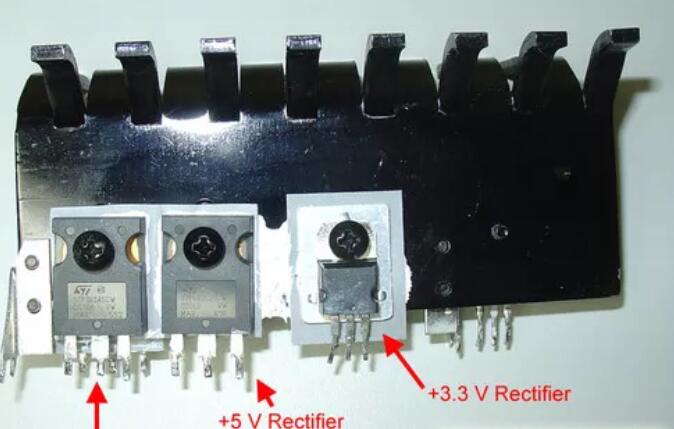
Components of secondary side of high-end power supply
Components of secondary side of high-end power supply
Here we can see:
Two parallel Schottky rectifiers for 12V output. Low-end power supply often has only one such rectifier. This design naturally doubles the maximum current output of the rectifier. This power supply uses two STPS6045CW Schottky rectifiers, each of which can run a maximum current of 60A.
☆ A Schottky rectifier responsible for 5V output. This power supply adopts STPS60L30CW rectifier, which can allow a maximum current of 60A to pass through.
☆ A Schottky rectifier responsible for 3.3V output, which is the main difference between high-end power supply and low-end power supply (the low-end power supply often does not have a separate 3.3V output). This power supply adopts STPS30L30CT Schottky, which can allow a maximum current of 30A to pass through.
☆ A voltage regulator of a power protection circuit. This is also a symbol of high-end power supply.
The main point is that the maximum current output mentioned above is only relative to a single component. The maximum current output of a power supply actually depends on the quality of many components connected to it, such as coil inductance, transformer, wire thickness, width of PCB and so on. We can get the theoretical maximum power of the power supply by multiplying the maximum current of the rectifier and the output voltage. For example, the 12V output maximum power of the power supply in the last figure should be 16A*12V=192W.
Disclaimer: This article is reproduced from the "Power R&D Elite Circle" to support the protection of intellectual property rights. Please indicate the original source and author of the reprint. If there is any infringement, please contact us to delete it.


Site Map | 萨科微 | 金航标 | Slkor | Kinghelm
RU | FR | DE | IT | ES | PT | JA | KO | AR | TR | TH | MS | VI | MG | FA | ZH-TW | HR | BG | SD| GD | SN | SM | PS | LB | KY | KU | HAW | CO | AM | UZ | TG | SU | ST | ML | KK | NY | ZU | YO | TE | TA | SO| PA| NE | MN | MI | LA | LO | KM | KN
| JW | IG | HMN | HA | EO | CEB | BS | BN | UR | HT | KA | EU | AZ | HY | YI |MK | IS | BE | CY | GA | SW | SV | AF | FA | TR | TH | MT | HU | GL | ET | NL | DA | CS | FI | EL | HI | NO | PL | RO | CA | TL | IW | LV | ID | LT | SR | SQ | SL | UK
Copyright ©2015-2025 Shenzhen Slkor Micro Semicon Co., Ltd
