Service hotline
+86 0755-83044319

release time:2022-03-17Author source:SlkorBrowse:12251
1、Critical loop and critical nodes of BUCK convert
No matter what type of converter it is, the key of PCB layout design is to find the key circuits and key nodes of the circuit system. So what are the key circuits and key nodes of the circuit system? Generally, the loop with large current change rate di/dt and the node with large voltage change rate dV/dt are the key loops and key nodes, which should be given priority in PCB layout design.
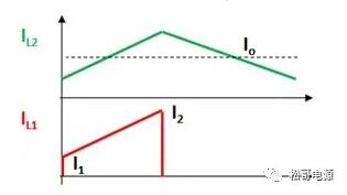
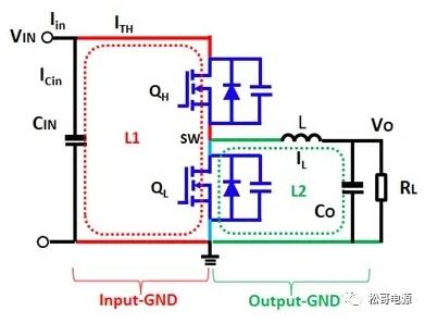
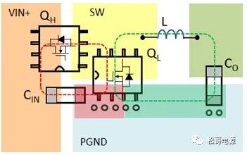
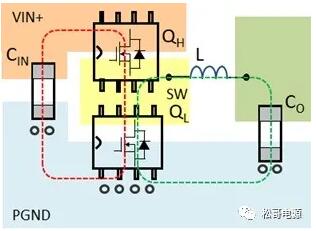
When the upper tube of BUCK converter is turned on and off, the current and waveform of each loop are shown in Figure 1.
(a)上管开通的电流回路
(b)上管关断的电流回路
(c)L1和L2环路的电流波形
(d)开关节点SW工作电压
(e)BUCK的工作电流环路
图1:BUCK的工作电流环路及波形
If L1 is called the input loop, L2 is called the output loop; The S source of the lower tube to the ground of the input capacitor is called the input ground, and the S source of the lower tube to the ground of the input and output capacitor is called the output ground. It can be found that:(1) The current in
1)L1 loop, including the input ground, is a pulse current waveform. The leading edge and the trailing edge of the current waveform have a very large current change rate di/dt.(2) The current of
2)L2 circuit, including the output ground, is equivalent to the direct current, and the alternating triangular wave with smaller peak-to-peak value is superimposed. The leading edge and trailing edge of the current waveform have smaller current change rate di/dt.
Therefore, the input loop with a very large current change rate di/dt, that is, the L1 loop, including the input ground, is the interference source of strong magnetic field emission.
If you look at the voltage waveform, the input voltage, the output voltage and the ground circuit are all stable voltages, while the voltage of the switch node SW produces a very large voltage change rate dV/dt during the process of the upper tube opening and closing, which is the interference source of strong electric field emission.
2、Basic design and layout requirements of BUCK converter PCB
According to the working principle of BUCK converter, the current characteristics of each loop and the voltage characteristics of switch nodes, it is easy to get the basic principles of BUCK converter PCB layout:
(1) The input loop L1, including the input ground, should be as short as possible, that is, the positive terminal of the input capacitor CIN should be as close to the drain D of the upper tube as possible, and the ground terminal of the input capacitor CIN should be as close to the source S of the lower tube as possible. The wiring of the loop should be as thick as possible, so as to reduce the parasitic inductance of the loop and the magnetic field interference.If necessary, place a small-sized decoupling ceramic capacitor at the nearest distance between the drain D of the upper tube and the source S of the lower tube.The input circuit is as short as possible and the wiring is thick, which can reduce stray resistance and conduction loss, which is beneficial to heat dissipation.
(2) The output loop L2, including the output ground, has little magnetic field interference, but the output current is usually relatively large. It is necessary to reduce the loop as much as possible, and make the wiring as thick as possible to reduce stray resistance and conduction loss, which is also conducive to heat dissipation and improve the efficiency of the system. To a certain extent, the magnetic field interference can also be reduced.
(3) The area of the switch node SW should be as small as possible, so as to reduce the parasitic capacitance of the node and the electric field interference. However, this node should be paved with copper skin to strengthen the heat dissipation of power MOSFET. Therefore, it is necessary to strike a balance between heat dissipation and EMI (Electric Field Emission Interference) design, and when necessary, an absorption circuit should be added to reduce the voltage change rate.
Other considerations are:
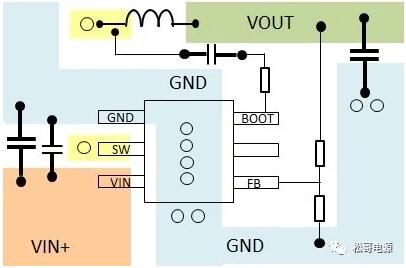
(4) All feedback signals and analog small signals should be kept away from the above circuits and nodes with large interference, and thinner wiring should be used as much as possible. Do not flow switching current under the control IC or converter. The current sampling signal should be connected in Kevin, and the RC filter network of the current sampling signal should be as close to the pins of IC as possible.

图2:电流取样信号
(5) The grounding of the input and output capacitors is connected to the ground plane of the bottom or inner layer through multiple vias. If the bottom of the device has copper skin with electrical characteristics of grounding, it can also be connected to the ground plane of the bottom or inner layer through multiple vias to enhance heat dissipation.
(6)DC power supply and DC ground, equivalent to AC ground, can shield interference signals, so do not divide them as much as possible. If segmentation is inevitable, reduce the number and length of signal lines as much as possible, and isolate small signals from large signal planes by AC as much as possible.
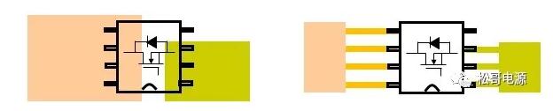
(7) The Gate gate drive loop of power MOSFET should be as short as possible, and parallel wiring should be used. The source D and drain S of MOSFET are wired with copper as much as possible, as shown in Figure 3.
(a) 好的布线 (b) 不好布线
图3:功率MOSFET的布线
(8) The power supply system of 2-layer board, the top layer is the component and power loop layer, and the bottom layer is the small signal and ground plane layer. 4-layer or 6-layer board, the following scheme can be adopted.
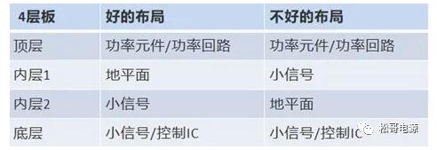
表1:4层板各层分配
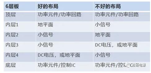
表2:6层板各层分配
3、Example of PCB design layout of BUCK converter
3.1Discrete scheme
The upper and lower tubes adopt discrete power MOSFET, and there are two common layouts of the upper and lower tubes:
(1) The upper pipe and the lower pipe are horizontal and vertical at 90 degrees, as shown in Figure 4;
(2) The upper pipe and the lower pipe are horizontally arranged, as shown in Figure 5.
The basic principle is: first lay out the main power circuit, especially the input capacitor and power MOSFET circuit, then lay out the inductor and output capacitor circuit, considering the division of power ground and small signal ground; Finally, on the small signal ground side, lay out the relevant signal lines.
(a) 优化布局
(b) 较差布局
图4:垂直排列分立器件BUCK布局
The two layouts in fig. 4, the input loop and the input ground in fig. 4(a), are much smaller than those in fig. 4(b), so the layout in fig. 4(a) is more optimized.
(a) 顶层布局

(b) 高频电容
(c) 高频电容放置背面底层
图5:水平排列分立器件BUCK布局
In the layout of Figure 5, Cin is far away, and the input loop and input ground are relatively large, but this layout is suitable for multi-tube parallel connection, and the current loop of BUCK circuit can be reduced by adding high-frequency filter capacitor on the back of PCB.
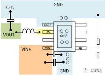
3.2 Integration scheme
The integration scheme refers to the BUCK converter IC that integrates the upper tube and the lower tube. The following designs come from the layout recommended by some manufacturers' device data sheets and the actual designs of some customer engineers.
The basic principle is the same as above: first lay out the main power circuit, especially the input capacitor and IC ground circuit, then lay out the output capacitor, considering the division of power ground and small signal ground; Finally, on the small signal ground side, lay out the relevant signal lines.
(a) 布局1
(b) 布局2
(c) 布局3
图6:SOT23几种PCB布局
According to the analysis method of fig. 4, the current paths of the upper tube on and off in fig. 6 are respectively drawn, and it can be found that:
(1) the current path in fig. 6(a) should pass through the bottom of the IC and return to the ground of the input capacitor below. the current path is long, and the power ground (the upper left corner area of the IC's GND pin) and the small signal ground (the right area of the IC's GND pin) should also be strictly divided. the advantage is that the switch node SW is directly connected to the inductor on the top floor.
(2) The current path in Figure 6(b) is the shortest, and the power ground (the upper left corner area PGND of IC's GND pin) and the small signal ground (the right area SGND of IC's GND pin) are strictly divided, as shown in Figure 7. The disadvantage is that the switch node SW is connected to the inductor through a via hole.
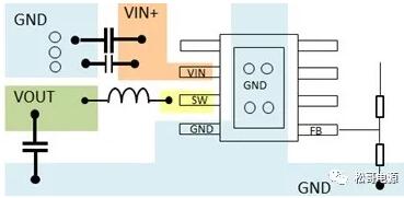
图7:SOT23布局2电流路径
(3) in fig. 6(c), the components near the right pin of the IC, a resistor and a capacitor connected to the BOOT pin make the ground of the output capacitor not directly return to the GND pin of the IC. There are two circuits for the connection between the ground of the output capacitor and the GND pin of the IC: one is through the via hole at the bottom of the IC, the via hole near the ground of the output capacitor, and the ground plane at the bottom to form a connection circuit; The other is the ground of the output capacitor, which is wound from under the IC to the GND pin of the IC and the ground of the input capacitor through the top copper skin.In this layout design, the current path is the longest, the power ground and the small signal ground are not partitioned, and the switch node SW is connected to the inductor through the via hole, so the layout design is poor.At the bottom of SOT23 device, there is a copper skin with electrical characteristics grounded. On the corresponding pad of PCB, multiple vias can be laid, which can be connected to the ground plane of the bottom layer or the inner layer to enhance heat dissipation. As shown in Figure 8, under the permitted conditions, lay as many vias as possible, and the diameter of vias should be selected appropriately to ensure that after soldering, no tin will leak and tin will fill the vias.
图8:下部有铜皮SOT23 PCB布局
Figure 9 lists several PCB design layouts of SO8 package. Interested parties can analyze their advantages and disadvantages according to the above methods.
(a) 布局1
(b) 布局2
(c) 布局3
图9:下部有铜皮SO8几种PCB布局
Disclaimer: This article is reproduced from "Songge Power Supply" to support the protection of intellectual property rights. Please indicate the original source and author when reprinting. If there is any infringement, please contact us to delete it.


Site Map | 萨科微 | 金航标 | Slkor | Kinghelm
RU | FR | DE | IT | ES | PT | JA | KO | AR | TR | TH | MS | VI | MG | FA | ZH-TW | HR | BG | SD| GD | SN | SM | PS | LB | KY | KU | HAW | CO | AM | UZ | TG | SU | ST | ML | KK | NY | ZU | YO | TE | TA | SO| PA| NE | MN | MI | LA | LO | KM | KN
| JW | IG | HMN | HA | EO | CEB | BS | BN | UR | HT | KA | EU | AZ | HY | YI |MK | IS | BE | CY | GA | SW | SV | AF | FA | TR | TH | MT | HU | GL | ET | NL | DA | CS | FI | EL | HI | NO | PL | RO | CA | TL | IW | LV | ID | LT | SR | SQ | SL | UK
Copyright ©2015-2025 Shenzhen Slkor Micro Semicon Co., Ltd
