Service hotline
+86 0755-83044319

release time:2022-03-17Author source:SlkorBrowse:12373
Compared with LDO, the circuit of DC-DC is much more complicated, with higher noise and higher requirements for layout and layout. The quality of layout directly affects the performance of DC-DC, so it is very important to know the layout of DC-DC.
① Short switching circuit
The red LOOP1 in the figure below shows the current flow direction when the DC-DC high side tube is turned on and the low side tube is turned off; The green LOOP2 is the current flow direction when the high-side tube is closed and the low-side tube is opened;
To make these two circuits as small as possible and introduce less interference, the following principles should be observed:
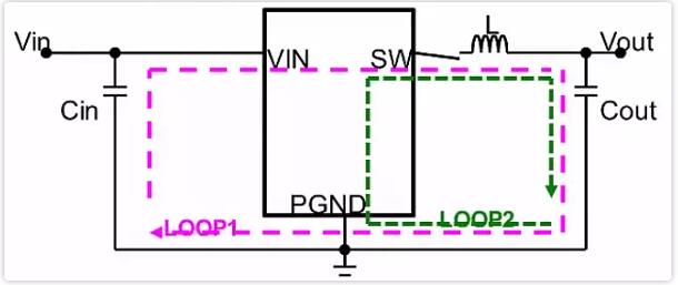
Why do you want to do this?
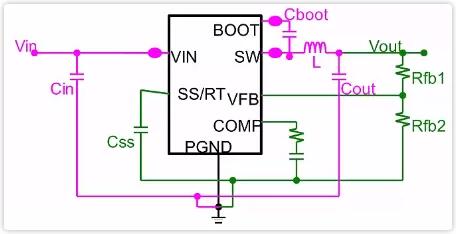
② Single point grounding
Single-point grounding refers to single-point grounding between signal ground and power ground. There will be relatively large switching noise on the power ground, so it is necessary to try to avoid interference to sensitive small signals, such as FB feedback pins.
The following diagram shows the layout of a development board of TI, with red as the current path when the upper tube is open and blue as the current path when the lower tube is open; The following layout has the following advantages:
① The GND of the input capacitor is connected with copper skin, and when decorating, the ground of the two should be put together as much as possible;The GND of the input capacitor is connected with copper skin, and when decorating, the ground of the two should be put together as much as possible;
②The current path of DC-DC Ton and Toff is very short;
③ The small signal on the right side is grounded at a single point, which is far away from the noise of the high current switch on the left side.
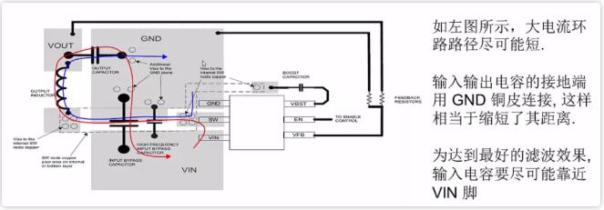 TI某开发板的DC-DC PCB layout
The layout of a typical DC-DC BUCK circuit is given as follows, and the following points are given in SPEC:
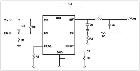
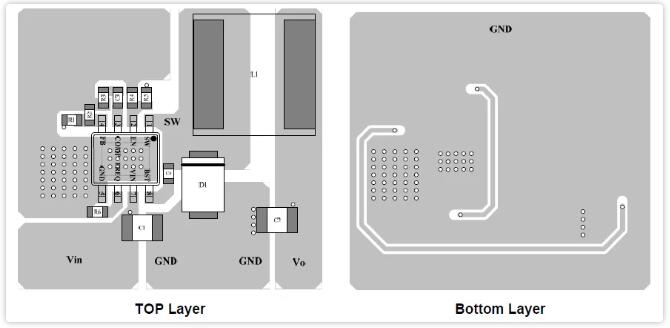
The layout of DC-DC circuit is very important, which directly affects the stability and performance of DC-DC. Generally, the SPEC of DC-DC chip will give layout guidance, which can be used for reference in design.
Disclaimer: This article is reproduced from "The Lion Attacking the City on Line 8". This article only represents the author's personal views, and does not represent the views of Sacco Micro and the industry. It is only for reprinting and sharing to support the protection of intellectual property rights. Please indicate the original source and author when reprinting. If there is any infringement, please contact us to delete it.
Company Tel: +86-0755-83044319
Fax/fax:+86-0755-83975897
Email: 1615456225@qq.com
QQ: 332496225 Manager Qiu
Address: Room 809, Block C, Zhantao Technology Building, No.1079 Minzhi Avenue, Longhua New District, Shenzhen


Site Map | 萨科微 | 金航标 | Slkor | Kinghelm
RU | FR | DE | IT | ES | PT | JA | KO | AR | TR | TH | MS | VI | MG | FA | ZH-TW | HR | BG | SD| GD | SN | SM | PS | LB | KY | KU | HAW | CO | AM | UZ | TG | SU | ST | ML | KK | NY | ZU | YO | TE | TA | SO| PA| NE | MN | MI | LA | LO | KM | KN
| JW | IG | HMN | HA | EO | CEB | BS | BN | UR | HT | KA | EU | AZ | HY | YI |MK | IS | BE | CY | GA | SW | SV | AF | FA | TR | TH | MT | HU | GL | ET | NL | DA | CS | FI | EL | HI | NO | PL | RO | CA | TL | IW | LV | ID | LT | SR | SQ | SL | UK
Copyright ©2015-2025 Shenzhen Slkor Micro Semicon Co., Ltd
