abstract
As a power supply R&D engineer, of course, I often come into contact with various chips. Some engineers may not be familiar with the inside of the chip. Many students go directly to the application page of data set when applying new chips, and build peripherals according to the recommended design. That's it. In this way, even if the application is fine, the technical details are ignored, and a better experience is not accumulated for your own technical growth. Today, taking the DC/DC step-down power supply chip LM2675 as an example, the internal design principle and structure of the following chips are explained in detail.
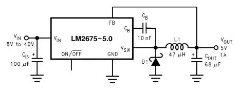
Typical application circuit of LM2675-5.0
 Open the DataSheet of LM2675, first look at the block diagram.
 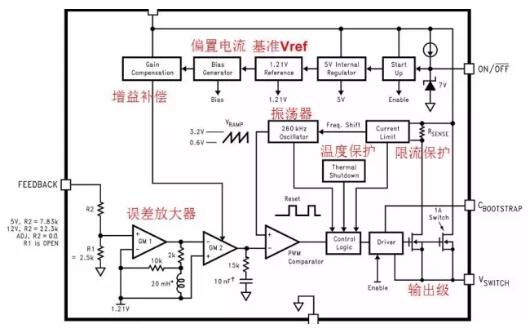 This diagram contains all the internal unit modules of the power supply chip. We have understood the BUCK structure well. The main function of this chip is to drive the MOS transistor, and to form a loop-controlled PWM drive power MOS transistor by detecting the output state of FB pin, so as to achieve stable voltage or constant current output. This is an asynchronous mode power supply, that is, the freewheeling device is an external diode, not an internal MOS tube.Let's analyze how each function is realized. 一、reference voltage
 Similar to the reference power supply of board-level circuit design, the internal reference voltage of the chip provides a stable reference voltage for other circuits of the chip. This reference voltage requires high precision, good stability and small temperature drift. The reference voltage inside the chip is also called bandgap reference voltage, because this voltage is close to the bandgap voltage of silicon, so it is called bandgap reference. This value is about 1.2V, as shown in the following figure:
 Let's go back to the textbook and talk about the formula, the current and voltage formula of PN junction:
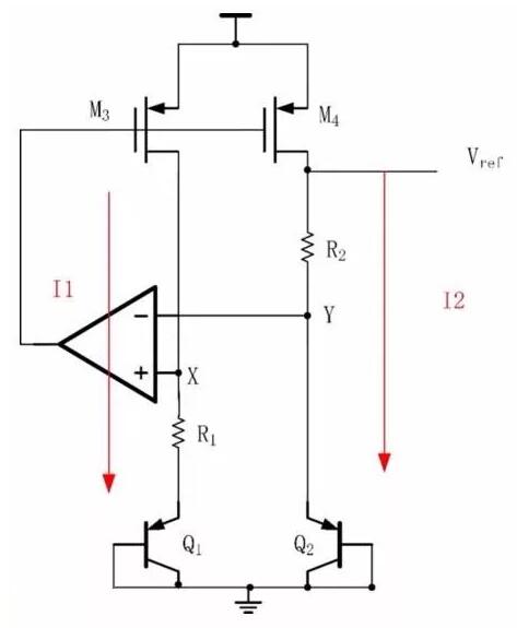
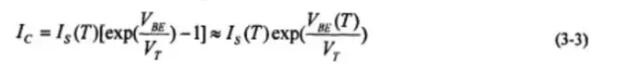 It can be seen that it Is exponential, and IS is reverse saturated leakage current (i.e. leakage current of PN junction caused by minority carrier drift). This current is proportional to the area of PN junction! Is->S ..In this way, Vbe=VT*ln(Ic/Is) can be deduced!Back to the figure above, according to the operational amplifier analysis, VX=VY, then it is I1*R1+Vbe1=Vbe2, so we can get: I1=△Vbe/R1, and because the gate voltages of M3 and M4 are the same, the current I1=I2, so the formula is derived: I1=I2=VT*ln(N/R1) N is the ratio of the PN junction areas of Q1 and Q2!Back to the figure above, according to the operational amplifier analysis, VX=VY, then it is I1*R1+Vbe1=Vbe2, so we can get: I1=△Vbe/R1, and because the gate voltages of M3 and M4 are the same, the current I1=I2, so the formula is derived: I1=I2=VT*ln(N/R1) N is the ratio of the PN junction areas of Q1 and Q2!In this way, we finally get the benchmark Vref=I2*R2+Vbe2. The key point is that I1 is a positive temperature coefficient, while Vbe is a negative temperature coefficient. After adjusting the value of N, it can achieve good temperature compensation! And a stable reference voltage is obtained. Generally, the industry designs according to 8. In order to achieve zero temperature coefficient, Vref=Vbe2+17.2*VT is calculated according to the formula, so it is about 1.2V At present, the benchmark of less than 1V can be achieved in the low-voltage field. Besides the temperature coefficient, there are problems such as PSRR suppression of power supply ripple, etc., which can't be deepened due to the level. The last diagram is like this, and the design of the operational amplifier is of course very particular:
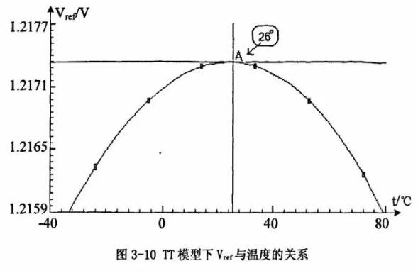
 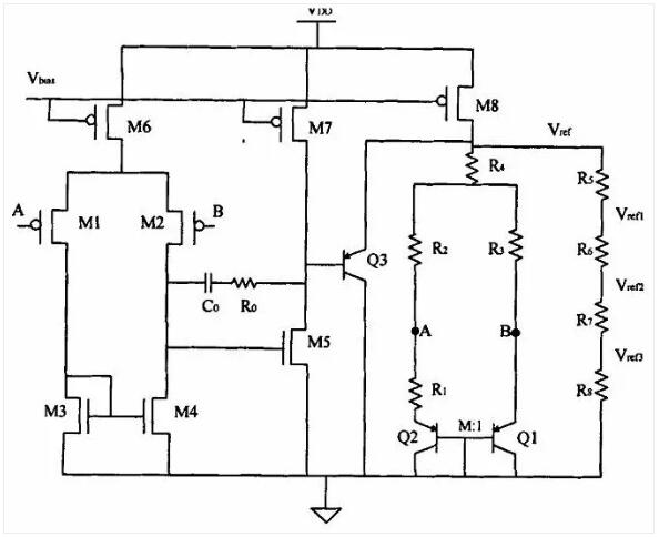 As shown in figure temperature characteristic simulation:
 二、Oscillator OSC and PWM We know that the basic principle of switching power supply is to use PWM square wave to drive power MOS transistor, so naturally, we need a module that generates oscillation. The principle is very simple, that is, the capacitor is charged and discharged to form sawtooth wave and the comparator is used to generate square wave with adjustable duty ratio.
 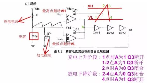 The final detailed circuit design is as follows:
 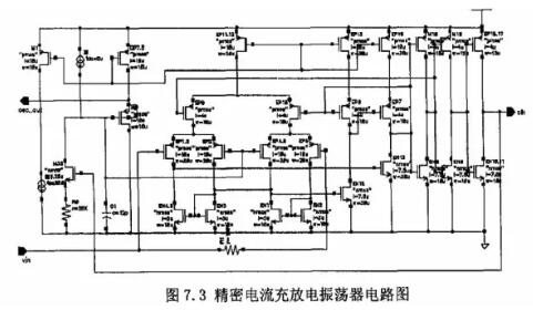 There is a technical difficulty in slope compensation in current mode, which is aimed at stabilizing the slope when the duty cycle is greater than 50%. I also have a superficial understanding, and interested students can study it in detail. 三、Error amplifier The function of error amplifier is to sample the feedback voltage to ensure the output constant current or constant voltage. Thereby adjusting the PWM of driving the MOS tube, as shown in the diagram:
 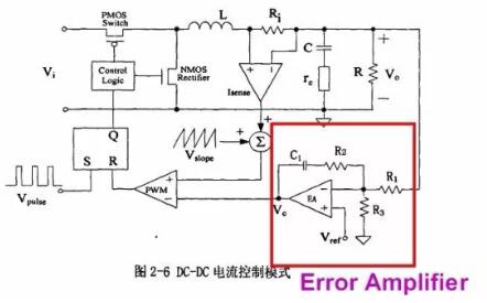 四、drive circuit The structure of the last driving part is very simple, that is, a large-area MOS tube with strong current capacity.
 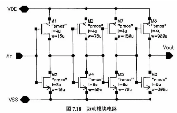 五、Other module circuits The other module circuits here are to ensure that the chip can work normally and reliably, although they are not the core of the principle, but they really occupy an important position in the design of the chip.Specifically, it has several functions: 1、Start module The function of the startup module is naturally to start the chip to work, because at the moment of power-on, it is possible that all transistor currents will be zero and remain unchanged, so it can't work. The function of starting the circuit is equivalent to "lighting a fire" and then turning it off. As shown in the figure:At the moment of power-on, S3 is naturally turned on, and then S2 can turn on M4 Q1, etc., so M1 M2 is turned on. The constant current source circuit on the right works normally, and S1 is turned on, so S2 is turned off, and the startup is completed. If there is no S1 S2 S3, the instantaneous current of all transistors is 0.
 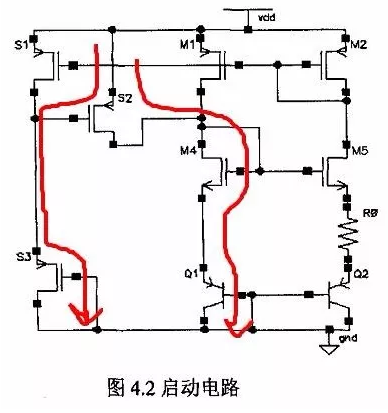 2、Overvoltage protection module OVP It is easy to understand that when the input voltage is too high, the output can be turned off by the switch tube to avoid damage, and a protection point can be set by the comparator.
 3、Overtemperature protection module OTP Temperature protection is to prevent the chip from being damaged by abnormal high temperature. The principle is relatively simple. The output is turned off by using the temperature characteristics of the transistor and then setting the protection point through the comparator
 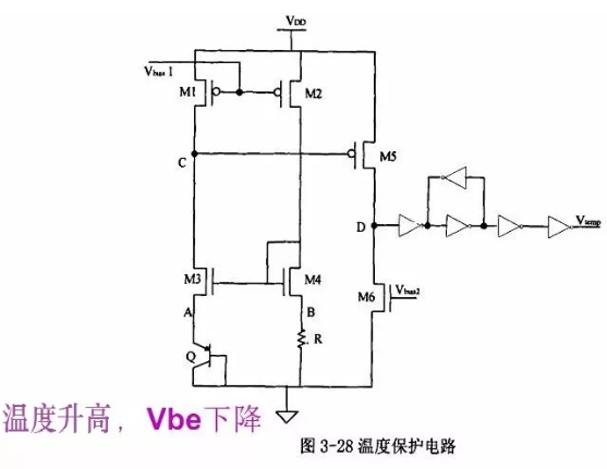 4、Overcurrent protection module OCP For example, when the output is short-circuited, the state of the output tube can be feedback controlled by detecting the output current, and the current can be turned off or limited. As shown in the figure, the current of the transistor is sampled in proportion to the area. Generally, the area of the sampling tube Q2 will be one thousandth of the area of the output tube, and then the driving of the MOS tube is controlled by the voltage comparator.
  There are some other auxiliary module designs
六、And constant current source and current mirror. Inside the IC, how to set the working state of each transistor is through bias current. Constant current source circuit can be said to be the cornerstone of all circuits, and band gap reference is also produced. Then, current mirror is used to provide current for each functional module. Current mirror is used to set the required current through the area of the transistor, which is similar to mirror image.
There are some other auxiliary module designs
六、And constant current source and current mirror. Inside the IC, how to set the working state of each transistor is through bias current. Constant current source circuit can be said to be the cornerstone of all circuits, and band gap reference is also produced. Then, current mirror is used to provide current for each functional module. Current mirror is used to set the required current through the area of the transistor, which is similar to mirror image. 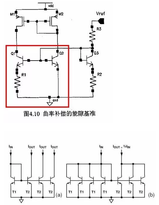 七、summarize
The above is probably the whole internal structure of the DC/DC power chip LM2675, and it is also a review of the previous fur knowledge. Of course, this is only the basic structure in principle. A specific design needs to consider a lot of parameter characteristics, a lot of analysis and simulation, and a deep understanding of semiconductor process parameters, because the manufacturing process determines many parameters and performance of transistors. I do. Defective or completely unusable. The whole chip design is also a complicated system engineering, which requires good theoretical knowledge and practical experience.
Disclaimer: This article is reproduced from "ittbank". This article only represents the author's personal views, and does not represent the views of Sacco Micro and the industry. It is only for reprinting and sharing to support the protection of intellectual property rights. Please indicate the original source and author when reprinting. If there is any infringement, please contact us to delete it.
Company Tel: +86-0755-83044319
Fax/fax:+86-0755-83975897
Email: 1615456225@qq.com
QQ: 332496225 Manager Qiu
Address: Room 809, Block C, Zhantao Technology Building, No.1079 Minzhi Avenue, Longhua New District, Shenzhen


