Service hotline
+86 0755-83044319

release time:2022-03-17Author source:SlkorBrowse:12580
Reveal the secret! How to turn sand into 99.9999999% purity silicon wafer?
High-purity monocrystalline silicon is the basic material for manufacturing various chips. The purity of semiconductor-grade silicon is extremely high, usually reaching 99.9% (7 to 9 9s after the decimal point, or even 12 9s), and it is single crystal, that is, the crystal lattice of silicon atoms faces uniformly.
Of course, the purity mentioned here generally only considers the purity without metal impurities, excluding impurities such as oxygen and carbon.

If you pay more attention to chips, you should know that these extremely pure monocrystalline silicon wafers are made from sand. Today, let's take a look at the specific manufacturing process. It's about the serious industrial silicon production process, which eliminates some various niche methods.
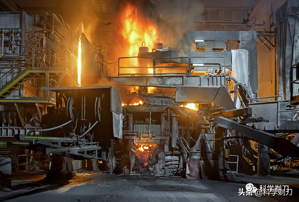
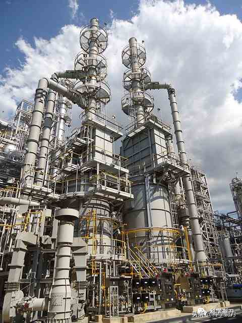
Usually carried out in a graphite electric arc furnace, quartzite (or sand) is mixed with coke, coal and sawdust, and heated to 1500 to 2000 degrees Celsius for carbothermal reduction reaction.
The specific reaction formula is shown in the above figure. The silicon produced in this step is called metallurgical silicon, and its purity can reach 96-99%. Metallurgical silicon is mainly used in aluminum alloy and silicone industry, and its purity can't reach the standard of semiconductor grade silicon, so it needs further purification.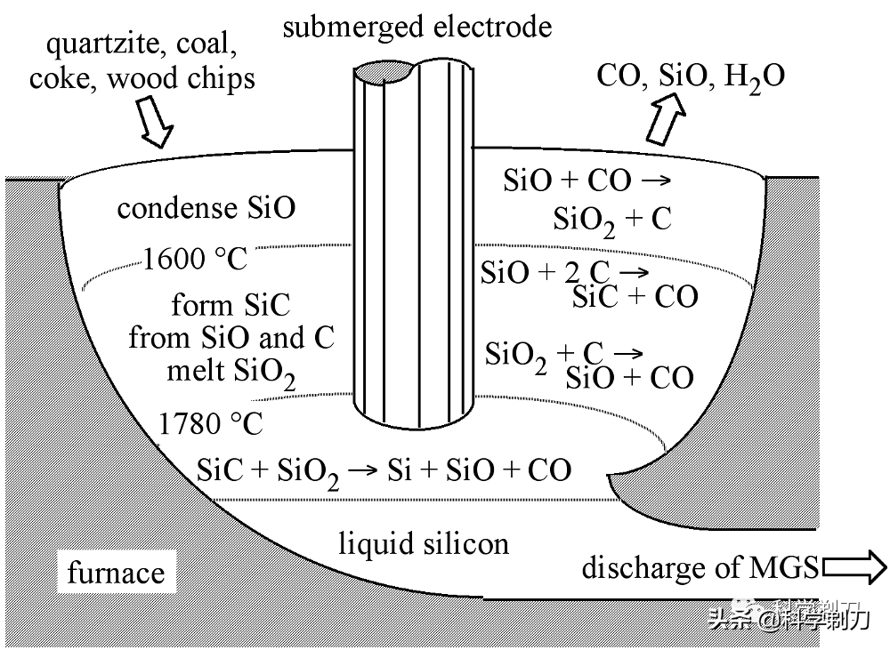
Of course, the above reaction equation is an overall process. In fact, a complex thermochemical reaction takes place in the graphite electric arc furnace. As shown in the above figure, intermediates such as silicon carbide and silicon monoxide are also produced during the reaction.
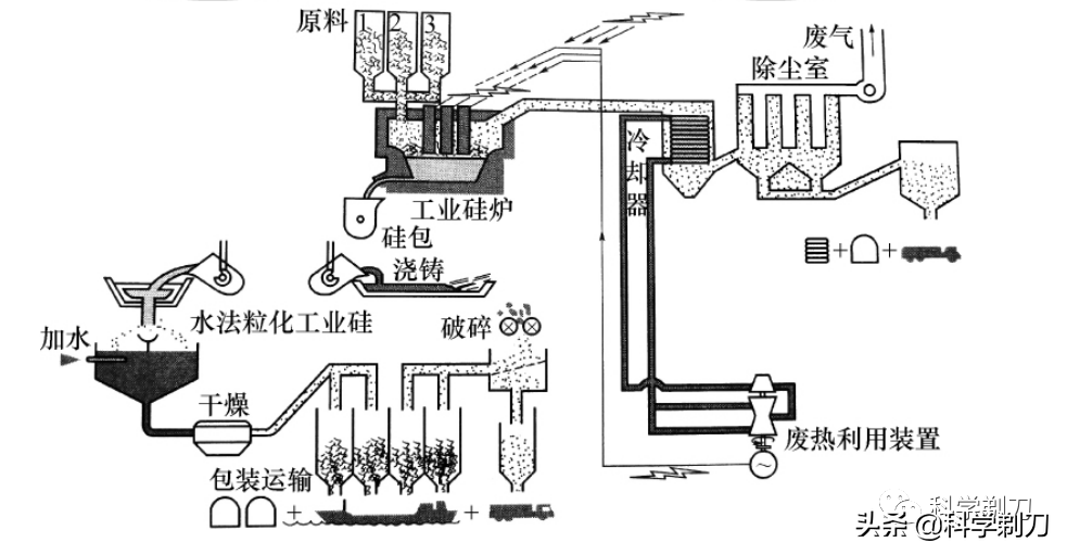
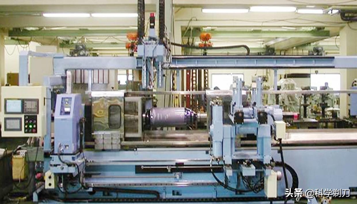
Large-scale enterprises generally use large-capacity electric furnaces, which have a high degree of mechanical automation such as raw material preparation, batching, feeding and motor pressing, and have an independent flue gas purification system. The picture above shows the production process of industrial silicon.
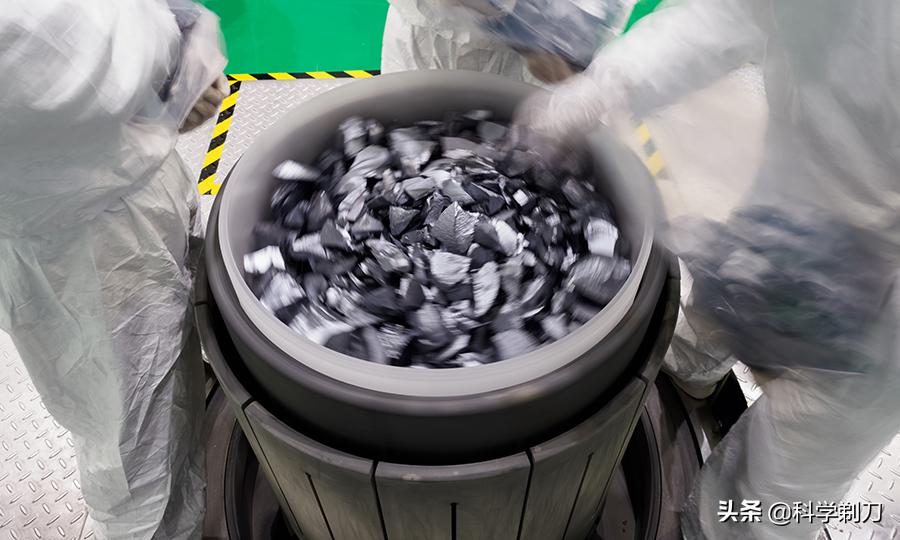
There are many ways to realize this step. Generally speaking, crude silicon should be purified by making it into halide or hydride, and then become high-purity silicon.
The existing methods mainly include trichlorosilane reduction method, silane thermal decomposition method, fluidized bed method and metallurgical method. At present, the main method of industrial scale production is trichlorosilane reduction method.
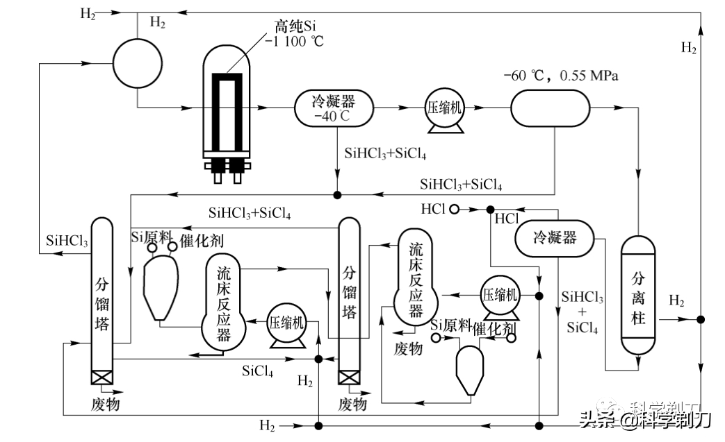
As shown in the above figure, the whole industrialization process was first invented by Siemens, so it is also called Siemens method. At present, there are 10 factories producing polysilicon all over the world, 70% of which come from Siemens process, and the whole process can be divided into three parts:
1. Synthesis of trichlorosilane.The reaction equation is shown above. SIlicon powder (Si) and hydrogen chloride (HCl), that is, hydrochloric acid, undergo catalytic synthesis reaction at 300℃ and 0.45 MPa to produce trichlorosilane (also called trichlorosilane or silicon chloroform), which is called chlorinated crude silicon.
2. Purification of trichlorosilane.
At present, there are perfect purification solutions in the industry. Generally, 5-9 towers are used for continuous purification. The total amount of trichlorosilane impurities purified by them is in the order of magnitude, which has reached the requirements of semiconductor purity, and the silicon produced by them does not need to undergo the first-class physical purification.
3. Hydrogen reduction reaction of trichlorosilane.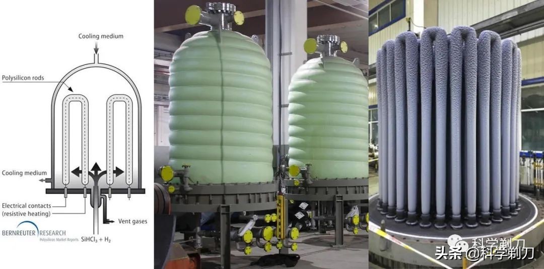
The reaction equation is as above. Using hydrogen as a reducing agent, hydrogen is bubbled into trichlorosilane liquid, so that high-purity silicon is deposited on a thin high-purity silicon rod with a temperature of 1100-1200 degrees (usually, a large current is applied to the thin pure silicon rod used for deposition to reach the required temperature), and the diameter of the produced polysilicon rod can reach 15-20cm. The hydrogen used for reduction must also be of high purity.
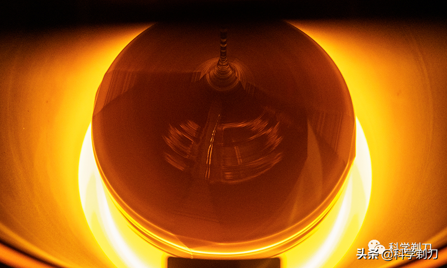
For the microelectronics industry, this is an extremely important step, from polycrystalline to single crystal. In essence, it is to change the random arrangement of silicon atoms from liquid phase to ordered array, and from asymmetric structure to symmetric structure. However, this transformation is accomplished by the movement of solid-liquid interface, which determines that monocrystalline silicon grows from molten polycrystalline silicon, and the crucible Czochralski method is the most widely used method. This method, also known as CZ method, is a crystal growth method established in 1917, referred to as CZ method for short.
The basic process is as follows:
Firstly, the polycrystalline silicon block and dopant are put into a Shi Ying crucible in a single crystal furnace to keep the temperature above 1420 degrees Celsius.
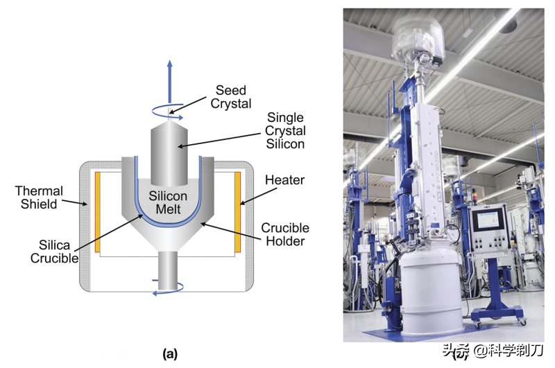
Then, a single crystal silicon rod (called seed crystal) with a very fine diameter (usually only 1CM) is placed in it. By controlling the temperature, the silicon atoms will form regular crystals along the silicon atom arrangement structure of the seed crystal at the solid-liquid interface between the molten polysilicon liquid and the single crystal silicon rod.
By rotating the seed crystal up a little, at this time, more silicon atoms will continue to deposit on the previous single crystal layer. As long as the environment is stable, crystals can be formed in a cycle, and finally a cylindrical silicon single crystal with neatly arranged atoms will be formed. Namely a silicon single crystal ingot.
Controlling the diameter and ensuring the growth of crystal with equal diameter is an important link in single crystal manufacturing. When the crystallization is accelerated, the diameter of the crystal will become thicker, increasing the speed of crystallization can make the diameter smaller, and increasing the temperature can inhibit the crystallization speed. On the contrary, if the crystallization slows down and the diameter becomes smaller, it can be controlled by reducing the drawing speed and temperature.
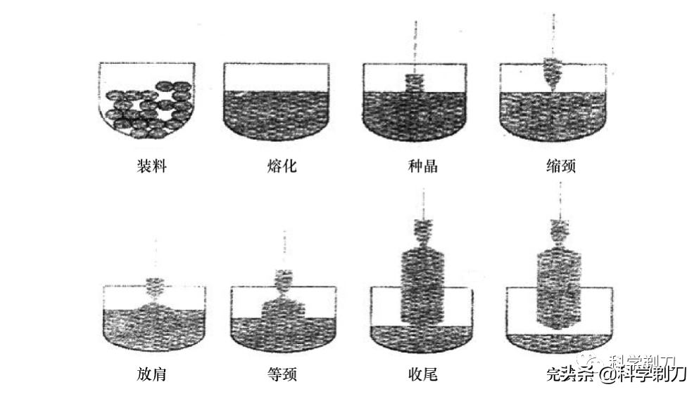
At the beginning of crystal pulling, a thin neck with a diameter of 3 ~ 5 mm is drawn to eliminate crystal dislocation. This process is called seeding. Then enlarge the diameter of single crystal to the technological requirements, and enter the equal diameter stage until most of the molten silicon is crystallized into single crystal ingot, leaving only a small amount of leftover materials.
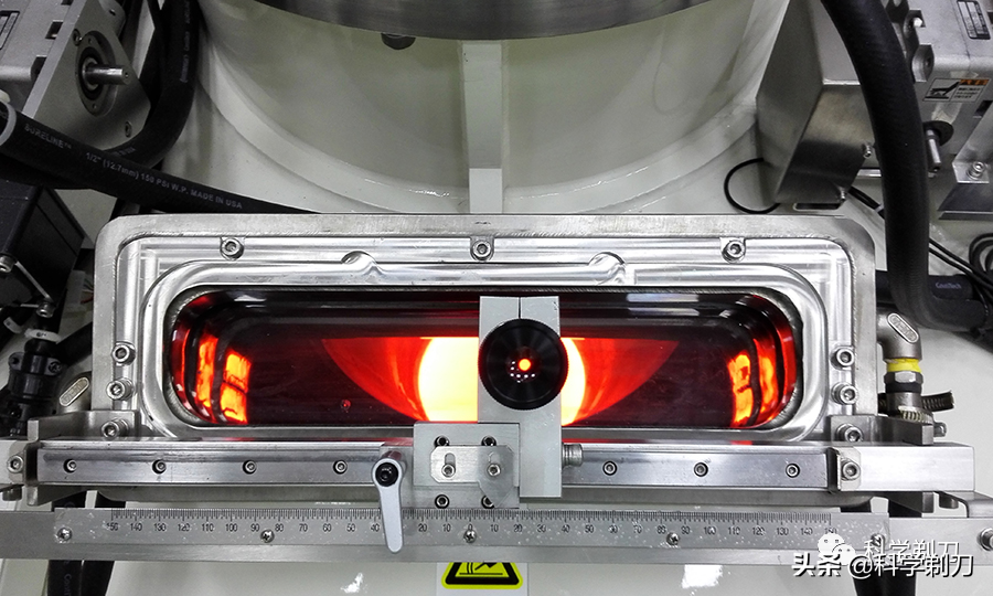
The melting point of silicon is about 1450℃, and the whole process of crystal pulling begins.Keep it at high temperature and negative pressure. The diameter measurement must be realized outside the crystal pulling furnace through the observation window in a non-contact way.
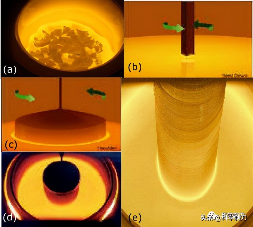
In the process of crystal pulling, a bright halo with high brightness will be formed at the junction of solid crystal and liquid melt, which is called aperture. Actually, the aperture is the reflection of the bright light from the crucible wall by the meniscus at the solid-liquid interface. When the crystal becomes thicker, the aperture diameter becomes larger, and vice versa. The change of single crystal diameter can be reflected by detecting the change of aperture diameter.
The whole process seems to be very simple, but in fact, there are as many as 13 steps in the project, and each step involves a lot of operation details. At the same time, with the iteration of technology and process, on the basis of Czochralski method, the magnetic field Czochralski method and continuous feeding process have been developed, so I won't repeat them here.
Simply put, it is to cut a monocrystalline silicon ingot into pieces of silicon wafers.
The processing procedures of silicon wafers used for semiconductors and solar panels are slightly different. Generally, a series of processes such as cutting, rounding, slicing, chamfering, grinding, chemical etching and polishing are required for single crystal silicon rods, and chemical cleaning with different procedures is interspersed among them.
Let's talk about the most important step: slicing.
Generally, internal circular cutting machine and wire cutting machine are used for slicing.
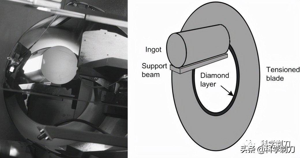
The internal cutting machine uses a kind of annular blade. The inner edge of the hollow annular blade is made of granular diamond, and the silicon block is placed in the middle ring to move back and forth. This embracing cutting method is more stable than the usual chainsaw cutting method, but this method consumes a lot of energy and damages the silicon wafer.
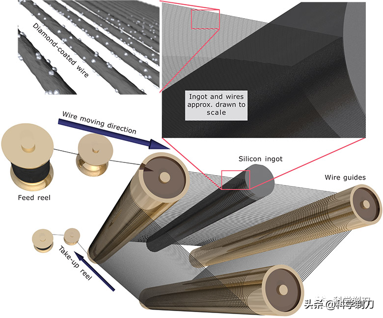
The other method is wire cutting, which achieves the purpose of cutting by the movement of a metal wire with diamond (about 180 microns in diameter). This method produces little stress and damages the silicon wafer, but the flatness of the silicon wafer produced by cutting is slightly poor (with big fluctuations). Wire cutting is usually mainly used for solar cells with low flatness requirements.
Ok, for the semiconductor industry, the whole process from sand to silicon wafer is almost finished.
Disclaimer: This article is reproduced from "Scientific Razor". This article only represents the author's personal views, and does not represent the views of Sacco Micro and the industry. It is only for reprinting and sharing to support the protection of intellectual property rights. Please indicate the original source and author when reprinting. If there is any infringement, please contact us to delete it.
Company Tel: +86-0755-83044319
Fax/fax:+86-0755-83975897
Email: 1615456225@qq.com
QQ: 3518641314 Manager Li
QQ: 332496225 Manager Qiu
Address: Room 809, Block C, Zhantao Technology Building, No.1079 Minzhi Avenue, Longhua New District, Shenzhen


Site Map | 萨科微 | 金航标 | Slkor | Kinghelm
RU | FR | DE | IT | ES | PT | JA | KO | AR | TR | TH | MS | VI | MG | FA | ZH-TW | HR | BG | SD| GD | SN | SM | PS | LB | KY | KU | HAW | CO | AM | UZ | TG | SU | ST | ML | KK | NY | ZU | YO | TE | TA | SO| PA| NE | MN | MI | LA | LO | KM | KN
| JW | IG | HMN | HA | EO | CEB | BS | BN | UR | HT | KA | EU | AZ | HY | YI |MK | IS | BE | CY | GA | SW | SV | AF | FA | TR | TH | MT | HU | GL | ET | NL | DA | CS | FI | EL | HI | NO | PL | RO | CA | TL | IW | LV | ID | LT | SR | SQ | SL | UK
Copyright ©2015-2025 Shenzhen Slkor Micro Semicon Co., Ltd
