Service hotline
+86 0755-83044319

release time:2022-03-17Author source:SlkorBrowse:12199
At the launching ceremony of "Chasing Light Lab" in Shanghai, Shen Bo, president of ASML (ASML) in China, said with a smile, with the increasing social attention of semiconductors in recent years, ASML has successfully gone out of the circle, from being an invisible champion only known by people in the industry to being a online celebrity company that the whole people can talk about. Reports and topics related to ASML can be seen almost every day. Gao Weimin, technical director of ASML China, even summed up the description of ASML in media reports. He said that the visual description of professional media is impressive, which makes the public understand well and the professionalism is in place.
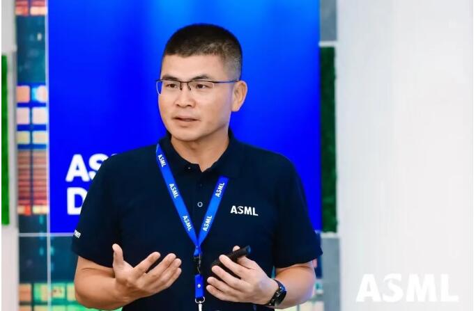
Shen Bo, President of ASML China
But after all, mask aligner is extremely complicated and exquisite, and has the reputation of being the most complicated and precise instrument of mankind, so it is difficult to interpret it all by visual description. In order to let the professional audience have a deeper understanding of mask aligner's principle, Gao Weimin gave a technical lesson to the participating media.
Mask aligner workflow
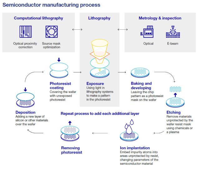
The semiconductor manufacturing process is very long, and the former manufacturing process can be roughly divided into seven links, namely, gluing, photolithography, baking, etching, ion implantation, glue removal and deposition. Lithography is one of the seven links and the most important one, which directly determines the size (i.e., process node) and yield of transistors that can be processed in the semiconductor production line. According to the data collected by Southwest Securities, the lithography process takes 40% to 50% of the whole wafer manufacturing process, and the lithography process cost accounts for about 30% of the chip generation cost.
Source: ASML Annual Report
According to Gao Weimin, there are three kinds of equipment working together in lithography, namely, mask aligner, gluing developer and detector. The automated production line sends the wafers to be processed to the gluing and developing machine to be coated with photoresist. The wafers coated with photoresist are sent to the mask aligner for exposure. The exposed wafers need to be sent back to the gluing and developing machine for development. After the developed wafers pass the inspection of the detector, they will go to the next step. If the inspection fails, the wafers will be sent back for rework.

Gao Weimin, Technical Director of ASML China
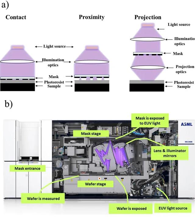
From the functional division, mask aligner can be roughly divided into several parts, such as light source, light channel, mask, projection objective and wafer processing area. At work, mask aligner made the mask pattern through the projection mirror, reduced it by four times and irradiated it on the wafer. The wafer coated with photoresist changed chemically, and then sent it back to the glue developing machine for development. In order to improve the productivity and the wafer movement speed is extremely high, mask aligner needs to complete the lithography in a high-speed dynamic state, and the control accuracy is within 1 to 2 nanometers. In order to ensure the high-precision lithography, mask aligner has built-in thousands of sensors, which control the lithography through a large number of parameter feedback. "This is a very, very difficult machine, an unimaginable precision instrument." Gao Weimin said.
Source: Network
在《ASML光刻机PK 原子弹,难度?》这篇文章中,就曾形象地描述:现在[敏感词]的EUV光刻机可以做到的“雕刻精度”是7nm,这相当于一根头发的万分之一。在雕刻的过程中晶圆需要被快速移动,每次移动10厘米,可是误差必须被控制在纳米级别。这种误差级别相当于眨眼之间端着一盘菜从北京天安门冲到上海外滩,恰好踩到预定的脚印上,菜还保持端平不能洒。
A formula dominates the world.
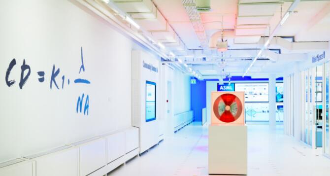
Mask aligner determines the size of semiconductor process, so what determines the processing accuracy of mask aligner? Gao Weimin introduced that ASML's innovation in lithography mainly started with Abbe's formula. Abbe's formula is the resolution formula of optical equipment, which can be found in prominent positions in every office of ASML: CD =K1*λ/NA. The formula shows that the minimum resolution size of optical system is related to three parameters, the first is wavelength (λ), the second is numerical aperture (NA), and the third is process factor or process factor (K1). That is, the smaller the wavelength, the smaller the size that can be resolved and the higher the resolution; The larger the digital aperture, the smaller the size that can be resolved and the higher the resolution. The smaller the process factor, the smaller the resolvable size and the higher the resolution.
Source: ASML Annual Report
Reducing the wavelength of light source is the main technical direction of mask aligner to improve machining accuracy. The wavelength of light source in mainstream mask aligner market has also been reduced from 436 nm (so-called g-Line) in 1980s to 13.5 nm extreme ultraviolet wavelength today. In the field of mask aligner, ASML was not as outstanding as it is now. In the era of g-Line(436 nm wavelength light source) and i-Line(365 nm wavelength light source), Japanese manufacturers had obvious advantages. After entering the 248 nm wavelength light source, ASML gradually caught up.
According to Gao Weimin, around 2003, ASML and other manufacturers in mask aligner also developed 157 nm light source, but the 157 nm light source was not put into commercial use because of inadequate supporting materials. On the contrary, every cloud has a silver lining and ASML developed immersion lithography technology on 193 nm light source, further expanding their leading edge over Japanese manufacturers.

Source: Network
Increasing the numerical aperture is another direction to increase the resolution. However, the lens size has a physical limit, and the lens size in mainstream mask aligner is already very large, so it is unrealistic to enlarge the lens in terms of cost and engineering realization. However, if the optical medium of the wafer is changed and the refractive index is increased, it is equivalent to enlarging the numerical aperture, which is the wetting principle.
Immersion mask aligner replaces the optical medium of the wafer with water from air, which increases the refractive index, thus improving the resolution.
Besides wavelength and numerical aperture, ASML has done a lot of research on light source optimization to improve mask aligner resolution. Lithography is an important technology of light source optimization, and ASML classifies it as K1 in Abbe formula, that is, process factor. For a given optical pattern, ASML mask aligner obtains the best illumination pattern by calculating the mask aligner technique, and sets the micromirror array to project the best illumination pattern onto the wafer for lithography, thus improving the processing accuracy.
Crossing the Gap from Theory to Engineering Realization
Abbe's formula is so concise, and Japanese manufacturers have accumulated a lot in the field of optics. So how did ASML win deus ex in the fierce competition? In Shen Bo's and Gao Weimin's explanations, we can probably get the answer, that is, attaching importance to R&D, being brave in trying, and having a mission.
Taking immersion lithography as an example, the principle is very simple, but the engineering implementation is extremely challenging. Only when the optical path medium is changed from air to water, several points should be considered: how to ensure that the water flowing through the photoresist will not produce impurities and bubbles, how to dissipate the heat generated by the high-speed friction between the water flow and the wafer, and how to homogenize the thermal field of the water flow. ......
Just how to place the water in the corresponding lithography position is a great technical problem. ASML used gas to stabilize water in the established lithography position, which skillfully solved this problem. However, it took ASML a lot of time to solve the technical problems such as how to make water flow in the gas, how to balance the air flow with the water flow, and how the water flow dissipates heat through the air flow.
In addition, immersion lithography needs to enlarge the lens size to meet the application requirements of water as optical medium. Gao Weimin said that it is quite different from the optical system of dry lithography, and the technological change of immersion lithography is far more complicated than the principle realization.
Double stage is another example. With the continuous improvement of semiconductor technology integration, the line width that can be processed is getting smaller and smaller. In order to ensure that the yield can still meet the requirements of mass engineering production, more and more parameter measurement and state monitoring are needed in the process of lithography in mask aligner. The increase of test parameters leads to the longer measurement time, which leads to the decrease of productivity. Parallel processing with double work tables is a solution given by ASML. On the double work tables, two wafers are entered at a time, one wafer is photoetched and the other wafer is tested. This can not only meet the requirements of advanced technology for testing and measuring in the processing process, but also improve the yield. According to Gao Weimin, compared with single workpiece table, the output rate of double workpiece table has increased by about one third. a hundred million
There are also many challenges in the engineering implementation of the double workpiece table. After adding a processing area, the diameter of the whole platform is about two or three meters. When such a large part moves at a high speed, it has to achieve nano-scale accuracy, which requires extremely high motion control and heat dissipation. ASML changed the previous pneumatic platform into a magnetic suspension platform, so that "big guys" can move flexibly.
Take promoting the development of the industry as its mission.
Nowadays, semiconductor manufacturing is approaching the physical limit. As the most critical link in the semiconductor manufacturing process, lithography technology has become the focus of the whole industry. ASML has been riding the dust in EUV lithography technology and exploring in no man's land for a long time. As Gao Weimin said, "How innovative ASML is determines what stage the industry can develop."
Industry progress depends on science and technology, and development of science and technology depends on talents. As an industry leader, ASML attaches great importance to talent development, with R&D investment accounting for 15% to 20% of sales. The 2020 financial report shows that ASML's R&D investment reached 2.2 billion euros, and there are more than 10,000 engineers worldwide. Among the more than 1,000 employees in China, the proportion of engineers is very high. ASML has two R&D centers in China. Shen Bo shared, "The achievements of ASML China in the past 20 years are attributed to our unique talent training system and the equal, respectful, inclusive and diverse environment created by ASML. In the process of helping employees to work and grow, employees can fully express their personal ideas, fully tap their potential here, and promote the iterative upgrading of innovative products and services, whether it is the strategic development of the project or career planning. "
In order to let China's top talents participate in the development of lithography technology, and to better support local customers in China, ASML will recruit hundreds of positions from all over the country, covering all the businesses of all-round lithography solutions, and provide positions such as customer service engineers, field application engineers and installation engineers in lithography equipment, computational lithography algorithm engineer, field application engineers and product engineers, as well as electronic engineers in measurement and inspection.
Shen Bo said that the mission of ASML is to liberate the potential of industrial development and push forward the technological limits. He said, "By exploring unprecedented technologies to solve the challenges faced by mankind, if we make progress, the semiconductor industry can't make progress."
Disclaimer: This article is reproduced from "SEMI Zhizao". This article only represents the author's personal views, and does not represent the views of Sacco Micro and the industry. It is only for reprinting and sharing to support the protection of intellectual property rights. Please indicate the original source and author when reprinting. If there is any infringement, please contact us to delete it.
Company Tel: +86-0755-83044319
Fax/fax:+86-0755-83975897
Email: 1615456225@qq.com
QQ: 3518641314 Manager Li
QQ: 332496225 Manager Qiu
Address: Room 809, Block C, Zhantao Technology Building, No.1079 Minzhi Avenue, Longhua New District, Shenzhen


Site Map | 萨科微 | 金航标 | Slkor | Kinghelm
RU | FR | DE | IT | ES | PT | JA | KO | AR | TR | TH | MS | VI | MG | FA | ZH-TW | HR | BG | SD| GD | SN | SM | PS | LB | KY | KU | HAW | CO | AM | UZ | TG | SU | ST | ML | KK | NY | ZU | YO | TE | TA | SO| PA| NE | MN | MI | LA | LO | KM | KN
| JW | IG | HMN | HA | EO | CEB | BS | BN | UR | HT | KA | EU | AZ | HY | YI |MK | IS | BE | CY | GA | SW | SV | AF | FA | TR | TH | MT | HU | GL | ET | NL | DA | CS | FI | EL | HI | NO | PL | RO | CA | TL | IW | LV | ID | LT | SR | SQ | SL | UK
Copyright ©2015-2025 Shenzhen Slkor Micro Semicon Co., Ltd
