Service hotline
+86 0755-83044319

release time:2022-03-17Author source:SlkorBrowse:10259
Let's talk about two questions today:
1. can the conduction current of MOS tube flow reversely? D to S, S to D direction is optional? 2. Can the MOS tube diode have too much current?
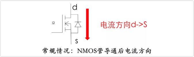
Why are there these two problems?When we first started to learn MOS transistors, we should all start with NMOS, and the current direction is from D to S.
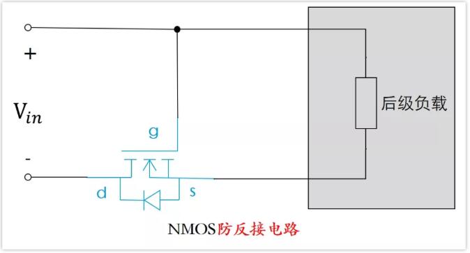
In practical applications, NMOS will have current from S to D, for example, the following NMOS transistor circuit for preventing reverse connection of power supply (only a schematic diagram, the actual circuit needs to consider some factors).
I'd better briefly explain the principle first.
1. When the power supply is connected normally
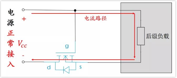
When the positive VCC is connected to the body diode through the rear load circuit, the body diode will conduct, and then the voltage of the S pole will be about 0.7V (the conducting voltage of the body diode).
At the same time, the gate g is connected to VCC, so Vgs=Vcc-0.7V>Vgsth, and the NMOS transistor is turned on. After the NMOS transistor is turned on, the on-voltage drop is basically 0, then Vgs=Vcc, and the MOS transistor remains on.
In this way, the whole power supply path is connected, the power supply supplies electricity to the rear load, and the rear circuit works normally.
Here, we need to pay special attention, that is, at this time, the current of MOS tube is S to D, which is opposite to D to S that we often see.
2、When the power supply is connected reversely (the power supply and the ground are connected reversely)
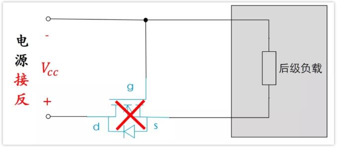
G is connected to the negative power supply, that is, 0V, and S is connected to the negative power supply through the load, that is, 0V, so Vgs=0V, and the MOS tube is not conductive.
At the same time, D is Vcc, S is 0V, and the body diode is reverse biased and non-conductive, so the current cannot flow through the NMOS tube.
For the load, the power supply is disconnected.
The reverse power supply won't reach the back load, so the back-stage circuit won't burn. As long as we connect the positive and negative poles of the front power supply, the back-stage circuit can work normally again, thus realizing the function of anti-reverse connection.
It needs to be said that the anti-reverse connection here does not mean that the power supply is connected in reverse, and the back-stage circuit can still work. Instead, the power supply is connected backwards, and the back-stage circuit will not smoke and burn out.
When I first saw this circuit before, I was actually drumming in my heart.
When this MOS tube is turned on, can the current flow backwards? D to S, S to D doesn't matter?

In addition to this current direction problem, there is also the problem of the body diode of the MOS tube. Can this diode have too much current?
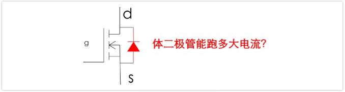
If you don't know, you will think that the current that this diode can flow is very small, because it also has a name called "parasitic diode", and it is easy to be deceived by it.The word "parasitic" can easily remind people of parasitic inductance and parasitic capacitance, and these two things are generally very small, so it is easy to mistake this parasitic diode for being too weak to pass a relatively large current.
trouble shooting
These two problems can actually be solved by one circuit, that is, the following BUCK circuit.
Everyone should know that the above circuit is a buck circuit. The lower tube is an NMOS tube. When the upper tube is off and the lower tube is on, the current of the inductor comes from the lower tube.
That is to say, the current direction of the down-transistor NMOS is from S to D, that is, the reverse current, and this current can be very large, because the current of the inductor can be relatively large, which is related to the load.
Besides, we also know from the previous article "Ringing Experiment and Analysis of BUCK" that there will be dead time (when the upper tube and the lower tube are not conducting) when the switch of BUCK is switched. The current of the inductor can't be broken, and the current of the inductor in dead time is the body diode of the down tube.
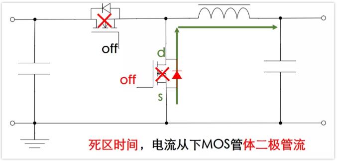
Because the current of the inductor depends on the load current, it can reach several amps, so the current of the body diode of the down tube can also be very large.
What is the maximum body diode current of MOS tube? Do you need to consider when selecting the type?
Many MOS transistors are not marked with this parameter, but some manufacturers do, such as this NMOS transistor SI9804.
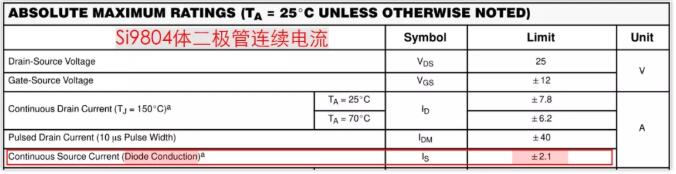
It can be seen from the above manual that the continuous current that can be passed is 2.1A
How did this come about?
I think this may be based on the power consumption limit.If the current time is short, a larger current can be passed;
if the time is long, the current cannot be too large.

As can be seen from the above figure, the maximum power consumption at 25℃ is 2.5W In this way, the continuous current mentioned above is 2.1A, which should also be based on the power consumption limit.
According to the conventional silicon diode, when a current of 2.1A flows, the on-voltage drop is about 1V, so the power consumption is P=2.1A*1V=2.1W, which is not much different from 2.5W.
Of course, the above is just my guess, and I haven't found any official statement.
A more detailed manual.
Writing here, I found a more detailed MOS transistor manual, Infineon's NMOS transistor BSC059N04LS6, which detailed the overcurrent capability of body diode, including continuous and instantaneous current.This manual convinced me of the above guess.
The following are the parameters of body diode in BSC059N04LS6 manual.
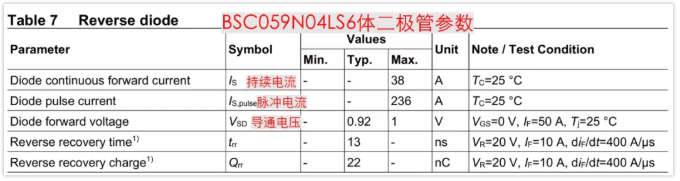
It can be seen directly from the above table that the continuous current of the body diode can reach 38A and the pulse current can reach 236A. At the same time, it can also be seen that the maximum conduction voltage of the diode is 1V.
May be a little surprised, this diode can keep current as high as 38A?
Actually, it can't be applied. We need to pay attention to the above condition, that is, Tc=25℃, and C is case, that is, when the shell is kept at 25℃.
In our practical application, if we don't add other heat dissipation measures, we can't guarantee that this MOS enclosure is at this temperature, and naturally, the current passing through 38A can't continue.
But it doesn't matter. We just look at the meaning of this parameter and want to know how it came from.
Let's look at the power consumption limits in the manual.

As you can see, at Tc=25℃, the power consumption limit is 38W. As we know earlier, the conduction voltage is 1V and the current limit is 38A, which is just the power consumption limit equal to the voltage multiplied by the current. What a coincidence.
Therefore, the current that the body diode can pass is based on the power consumption limit.
At the same time, we can see that at Ta=25℃, the power consumption limit is 3W, and this Ta is the ambient temperature, which should be closer to the actual use (without special heat dissipation measures).
If calculated with this value, then the current that the body diode can continuously pass through is about 3W/1V=3A. Of course, this is my guess, but it is not written in the manual.
At this point, at least we should know that the body diode can still pass a relatively large current. Of course, there is another problem. The above is about continuous current, and there must be the problem of instantaneous current. Can the instantaneous current be too large? This problem is even more important, because in normal use, we will not pass a long-lasting current to the body diode of MOS tube. If there is such a need, why don't we just turn on the MOS tube? The power consumption can be even lower. In the previous BUCK example, the current of the body diode only flows in the dead time, which is quite short. Therefore, it is more worthwhile to have a look at the excessive current in this moment. Let's look at the manual of BSC059N04LS6, because it's all marked out directly.
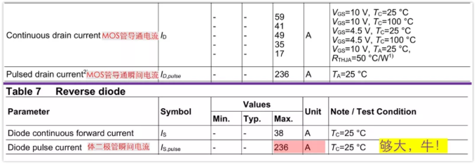
The conduction current of this tube can reach 59A, the current that can pass in 10us is 236A, and that of the body diode is 236A, both of which are the same, and both of them are very large, that is to say, the instantaneous current of the body diode will not become the bottleneck of use at all.
Maybe that's why we seldom pay attention to the current of the body diode of the MOS tube, only to see if the conduction current of the MOS tube is large enough.
To summarize the above contents:
1. After the MOS is turned on, the current can actually flow in both directions, from D to S, or from S to D. 2. The continuous current of MOS tube diode can be calculated according to the power consumption limit of MOS tube. 3. The current that MOS tube diode can pass instantly is equal to the current that NMOS tube can pass instantly after it is turned on, which is generally not the bottleneck.
Originally written here, the article can already be finished, but I still wonder if I can see the above content from the principle of MOS tube.
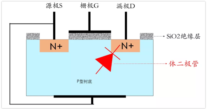
Here are some of my understandings for reference.Structure of NMOS tube
Let's take a look at the structure of NMOS transistor.
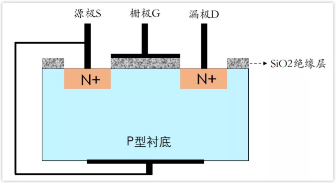
Take NMOS as an example. As shown above, S and D are N-type semiconductors with high doping concentration, and the substrate is P-type semiconductor, and the substrate and S pole are connected together.
When the Vgs voltage is greater than the mosfet Vth, that is, the gate is positively charged with respect to the substrate, it will attract minority carriers (electrons) from the P-type substrate to the P-type substrate, forming an inversion layer, that is, a conductive channel.
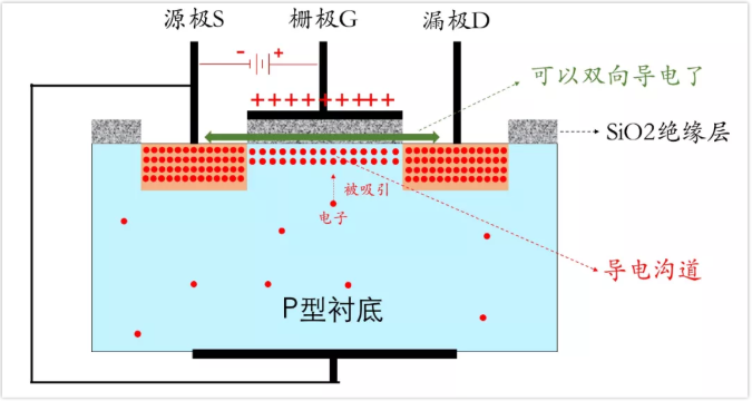
At this time, we will see that S and D are N-type semiconductors with many free electrons, and there are also many electrons between S and D, which can also conduct electricity.
That is to say, S and D are connected, and there are free electrons everywhere that can move.
Therefore, when we apply a voltage between s and d, a current will be formed, and no matter what the direction of the voltage is, as long as there is a voltage, a current can be formed, and there is no difference between the two.
That is to say, the current can flow in both directions, from D to S, or from S to D.
Let's look at the overcurrent capability of the body diode.
And p-type semiconductor are put together, a PN junction, that is, a diode, is always formed. The body diode between S and D is actually formed by the drain D and the substrate. Because S and the substrate are connected together, there is an individual diode between D and S.
The principle that the MOS tube is turned on is that the gate attracts minority carriers (electrons) in the P-type substrate, forming a conductive channel. This channel should also be relatively narrow, but it can already support the current of Id (the current when the MOS tube is turned on, each NMOS has this parameter).
Then, as a substrate with a large volume and area, it forms a PN junction with the drain, and the current naturally flowing through it reaches Id, so there is no problem (regardless of temperature).
However, because the formed channel resistance is very low, it doesn't generate much heat, and the PN junction always has a conduction voltage drop, and the current will generate heat, which is a big disadvantage, so the body diode is subject to this heating problem.
So the final result is that the continuous current flowing through the body diode is limited by the power consumption of the MOS transistor.
The above statement about the principle seems to be self-consistent and purely personal. If you have any questions, please correct me in the message area.
Disclaimer: This article is reproduced from "Chip House". This article only represents the author's personal views, and does not represent the views of Sacco Micro and the industry. It is only for reprinting and sharing to support the protection of intellectual property rights. Please indicate the original source and author when reprinting. If there is any infringement, please contact us to delete it.
Company Tel: +86-0755-83044319
Fax/fax:+86-0755-83975897
Email: 1615456225@qq.com
QQ: 3518641314 Manager Li
QQ: 332496225 Manager Qiu
Address: Room 809, Block C, Zhantao Technology Building, No.1079 Minzhi Avenue, Longhua New District, Shenzhen


Site Map | 萨科微 | 金航标 | Slkor | Kinghelm
RU | FR | DE | IT | ES | PT | JA | KO | AR | TR | TH | MS | VI | MG | FA | ZH-TW | HR | BG | SD| GD | SN | SM | PS | LB | KY | KU | HAW | CO | AM | UZ | TG | SU | ST | ML | KK | NY | ZU | YO | TE | TA | SO| PA| NE | MN | MI | LA | LO | KM | KN
| JW | IG | HMN | HA | EO | CEB | BS | BN | UR | HT | KA | EU | AZ | HY | YI |MK | IS | BE | CY | GA | SW | SV | AF | FA | TR | TH | MT | HU | GL | ET | NL | DA | CS | FI | EL | HI | NO | PL | RO | CA | TL | IW | LV | ID | LT | SR | SQ | SL | UK
Copyright ©2015-2025 Shenzhen Slkor Micro Semicon Co., Ltd
