Service hotline
+86 0755-83044319

release time:2022-03-17Author source:SlkorBrowse:11665
Basic concepts of failure analysisDefinition:
The process of diagnosing failed electronic components.
1. Failure analysis often requires electrical measurement and advanced physical, metallurgical and chemical analysis methods.
2. The purpose of failure analysis is to determine failure modes and failure mechanisms, and propose corrective measures to prevent the recurrence of such failure modes and failure mechanisms.
3. Failure mode refers to the observed failure phenomena and forms, such as open circuit, short circuit, parameter drift, function failure, etc.
4. Failure mechanism refers to the physical and chemical process of failure, such as fatigue, corrosion and overstress.
General procedure of failure analysis
1、Collect field data:

2、Measure and determine the failure mode.
Electrical measurement failure can be divided into connectivity failure, electrical parameter failure and functional failure.
Connection failure includes open circuit, short circuit and resistance change. This kind of failure is easy to test, and most of the field failures are caused by electrostatic discharge (ESD) and over-voltage stress (EOS).
Electrical failure requires complicated measurement, which is mainly manifested by parameter value exceeding the specified range (out of tolerance) and parameter instability.
To confirm the function failure, it is necessary to input a known excitation signal to the components and measure the output result. If the measured output state is the same as the expected state, the components function normally; otherwise, it is invalid, and the function test is mainly used for integrated circuits.
Three kinds of failures are related to each other, that is, one kind of failure may cause other kinds of failures. The root of functional failure and electrical parameter failure can often be attributed to connectivity failure. In the absence of complex functional testing equipment and testing procedures, it is possible to conduct electrical testing by simple connectivity testing and parameter testing methods, and satisfactory failure analysis results can still be obtained by combining the application of physical failure analysis technology.
3、Non-destructive inspection
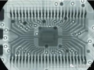
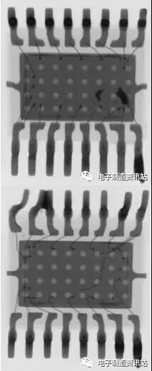
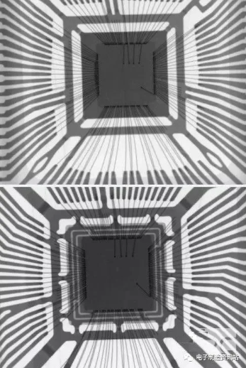
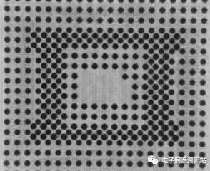
X-Ray inspection, that is, without damaging the chip, uses X-ray perspective of components (multi-direction and angle optional) to inspect the packaging conditions of components, such as bubbles, abnormal bonding lines, grain size, support direction, etc.
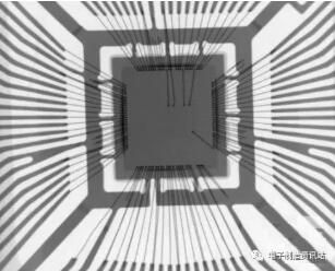
Applicable situation: Check whether there is abnormality in bonding, defects in packaging, and confirm grain size and layout.
Advantages: short construction period, intuitive and easy to analyze
Disadvantages: Limited access to information
Limitations:
1. For the same batch of devices, the internal shapes of devices in different packaging production lines are slightly different;
2. Internal line damage or defects are difficult to detect and must be obtained through functional tests and other tests.
Case analysis:
X-Ray flaw detection-bubbles and bonding lines
X-Ray authentication-blank ammunition (visible in the figure, no crystal grains)
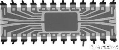
"Just what it looks like"
Here's the real thing
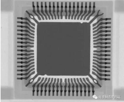
X-Ray is used for origin analysis (chips of the same brand and model in the following figure)
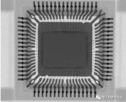
X-Ray is used for failure analysis (PCB flaw detection and analysis)
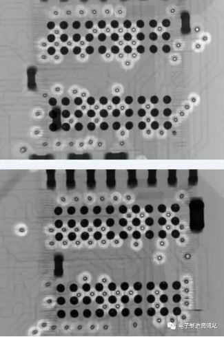
(The dense dot below is the solder bead of BGA. As we can see from the figure below, this chip is actually BGA secondary package)
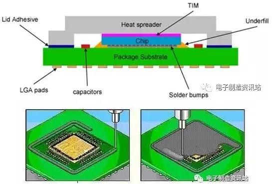
4、Open package
There are two methods of unsealing: mechanical method and chemical method. According to the packaging materials, the packaging types of microelectronic devices include glass packaging (diode), metal shell packaging, ceramic packaging and plastic packaging.Mechanical Kaifeng & Chemical Kaifeng
5、Microscopic image technique
Optical microscope analysis technology
Secondary electron image technology of scanning electron microscope
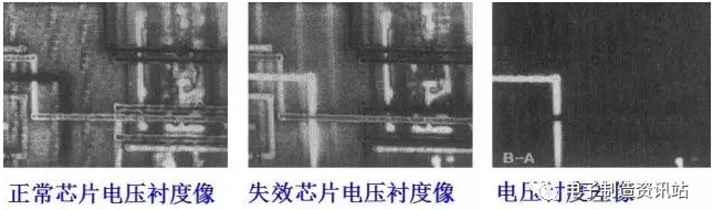
Failure location technology of voltage effect
6、Analysis of main failure mechanism of semiconductor
Electrical stress (EOD) damage
Electrostatic discharge (ESD) damage
Package failureWire bonding failure
Poor chip bonding
Metal semiconductor contact degradation
Sodium ion contamination failure
Pinhole failure of oxide layer
Disclaimer: This article is reproduced from "Electronic Production Information Station". This article only represents the author's personal views, and does not represent the views of Sacco Micro and the industry. It is only for reprinting and sharing to support the protection of intellectual property rights. Please indicate the original source and author when reprinting. If there is any infringement, please contact us to delete it.
Company Tel: +86-0755-83044319
Fax/fax:+86-0755-83975897
Email: 1615456225@qq.com
QQ: 3518641314 Manager Li
QQ: 332496225 Manager Qiu
Address: Room 809, Block C, Zhantao Technology Building, No.1079 Minzhi Avenue, Longhua New District, Shenzhen


Site Map | 萨科微 | 金航标 | Slkor | Kinghelm
RU | FR | DE | IT | ES | PT | JA | KO | AR | TR | TH | MS | VI | MG | FA | ZH-TW | HR | BG | SD| GD | SN | SM | PS | LB | KY | KU | HAW | CO | AM | UZ | TG | SU | ST | ML | KK | NY | ZU | YO | TE | TA | SO| PA| NE | MN | MI | LA | LO | KM | KN
| JW | IG | HMN | HA | EO | CEB | BS | BN | UR | HT | KA | EU | AZ | HY | YI |MK | IS | BE | CY | GA | SW | SV | AF | FA | TR | TH | MT | HU | GL | ET | NL | DA | CS | FI | EL | HI | NO | PL | RO | CA | TL | IW | LV | ID | LT | SR | SQ | SL | UK
Copyright ©2015-2025 Shenzhen Slkor Micro Semicon Co., Ltd
