Service hotline
+86 0755-83044319

release time:2022-03-17Author source:SlkorBrowse:10783
The development of high integration and miniaturization of electronic products, the high precision and miniaturization of electronic packaging, and the fine wiring and tiny aperture caused by high-density interconnection of PCBA have put forward stricter requirements for detection methods and technologies. Slice analysis technology is widely used in microscopic inspection of electronic products and plays an important role!
It is usually used as the basis for objective inspection, research and judgment, such as quality judgment and quality abnormality analysis of electronic products, quality inspection of PCB, PCBA welding quality inspection, finding the cause and solution of failure, and evaluating process improvement.
In the process of microstructure analysis, slice analysis is a very important analysis method. First of all, let's know what section analysis is, its form, detection steps and uses.
Slice analysis
Metallographic sectioning technology is a failure analysis technology, which uses special liquid thermosetting resin to embed and seal the samples, grinds and polishes the embedded samples, and then observes and detects the profile of the samples under a metallographic microscope.
Formal classification
According to the grinding direction, the slices are divided into vertical slices and horizontal slices.
1. Vertical sectioning means cutting along the direction perpendicular to the board surface, and observing the profile. Vertical sectioning is the most commonly used method in sectioning analysis.
2. The horizontal slice is ground down layer by layer along the overlapping direction of the board, which is used to observe the condition of each level, and is usually used to assist the vertical slice in analyzing and judging the quality abnormality.
Before starting the experiment, we need to make a preliminary judgment to choose which type of slicing method to perform, so as to find the problem more quickly and accurately.
According to standard
IPC-TM 650 2.1.1, IPC-TM 650-2.2.5 , IPC A 600, IPC A 610等。
main application
1. Sliced samples are usually observed by stereomicroscope or metallographic microscope;
2. The morphology and composition of the sliced sample can be observed by SEM/EDS scanning electron microscope and energy spectrum.
3. After nondestructive testing, such as X-ray and C-SAM samples, the suspected abnormal cracking and foreign body embedding can be observed and verified by slicing;
4. The sliced sample can be combined with FIB to make a more subtle micro-incision observation.
Chip analysis is widely used in PCB and SMT industries, which can effectively monitor the internal quality of products, find out the causes of problems and help solve them.It is suitable for PCB quality inspection and process improvement, electronic component structure analysis, PCBA welding reliability evaluation, solder joint tin form and defect detection, etc.
Then, how is the slice analysis technology applied to the detection of micro-defects and the observation of micro-structure of electronic products? Next, we will answer in detail and attach a typical case diagram!
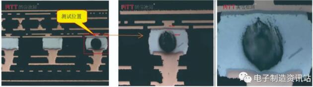
一、Observation of Micro-surface or Internal Structure Defects of Electronic Products
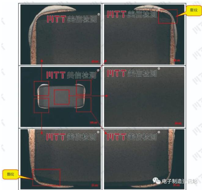
Observation on structural defects of electronic components and PCB. Slice method can be used to enlarge and observe small samples to detect holes, pinholes, blow holes, cracks and other defects in key positions of electronic components. Detect PCB delamination, hole copper fracture and other defects.
Typical case diagram
(Chip capacitor cracking failure)
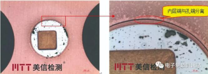
(PHT inner layer copper separation)

(PCB inner layer structure cracks)
二、PCB/PCBA welding detection
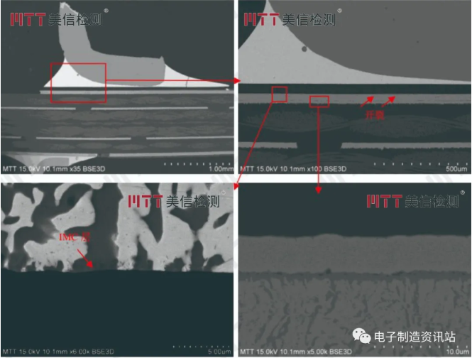
①BGA empty soldering, virtual soldering, hole, bridge, tin area, etc.;
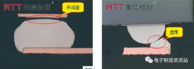
(BGA solder ball dummy solder/dummy solder)
② Check the thickness, layer number, through hole diameter and through hole quality observation of PCB, which is used to check the internal cavity of PCB solder joint, interface bonding condition, wetting quality evaluation, etc. Such as: analysis of capacitor and PCB copper foil layers, LED structure analysis, electroplating process analysis, internal structural defects of materials, etc.
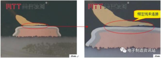
(The binding wire in the LED lamp is not connected)
(PCBA solder joints are well wetted with obvious holes)

(Observation of solder hole of camera substrate)
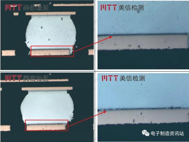
(Bonding Status of Main Board Welding Interface)
③ Micro-size measurement (generally greater than 1μm): pore size, tin plating height, copper foil thickness, etc.
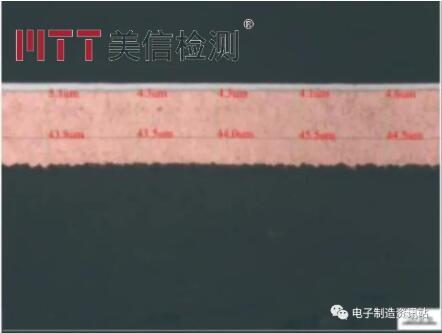
(PCB copper layer thickness)
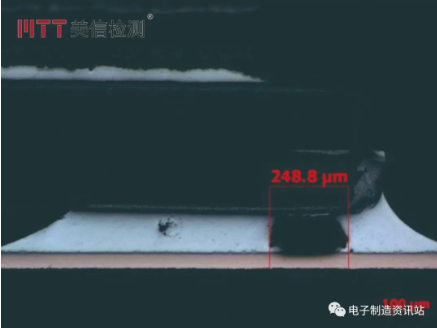
(solder hole size)
三、It is an important link in the failure analysis of electronic products.
1. Observe and analyze the quality of a single sample, find product problems, and make corresponding improvements.
2. Different batches, the same batch and different models of products fail. Through slice analysis, we can understand the failure mechanism of products, find out the causes of failure, and find the corresponding solutions to improve the yield and reduce the loss.
Typical case
After a PCBA is assembled, there are some bad phenomena such as LED devices falling off and parts falling off.
In order to find the root cause of the failure, we compared and analyzed the failed samples provided by customers with the OK samples, and made detailed analysis through visual inspection, surface analysis, slice analysis, simulation verification, AES analysis and other test items.
Among them, slicing analysis is to slice NG sample and OK sample respectively to understand the interface state of solder joints, and then observe and analyze the two samples by SEM+EDS, and draw the conclusion:
The direct cause of failure solder joint cracking in NG sample is that a good IMC layer cannot be formed between solder and nickel layer, which makes the interface of solder joint crack easily under stress.
(Slice analysis of NG samples)
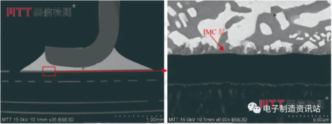
(section analysis of OK samples)
To sum up, we can know that the failure modes of products can be detected intuitively and accurately by metallographic section analysis, and the internal potential defects can be found in time to prevent the problems from enlarging and the waste of resources. Metallographic slice analysis is used to monitor the production process, which is not only used to detect solder joints after reflow, but also to monitor incoming materials, so as to find out whether the specifications of incoming materials meet the standards in time, so as to prevent the production of defective products.
Disclaimer: This article is reproduced from "Electronic Production Information Station". This article only represents the author's personal views, and does not represent the views of Sacco Micro and the industry. It is only for reprinting and sharing to support the protection of intellectual property rights. Please indicate the original source and author when reprinting. If there is any infringement, please contact us to delete it.
Company Tel: +86-0755-83044319
Fax/fax:+86-0755-83975897
Email: 1615456225@qq.com
QQ: 3518641314 Manager Li
QQ: 332496225 Manager Qiu
Address: Room 809, Block C, Zhantao Technology Building, No.1079 Minzhi Avenue, Longhua New District, Shenzhen


Site Map | 萨科微 | 金航标 | Slkor | Kinghelm
RU | FR | DE | IT | ES | PT | JA | KO | AR | TR | TH | MS | VI | MG | FA | ZH-TW | HR | BG | SD| GD | SN | SM | PS | LB | KY | KU | HAW | CO | AM | UZ | TG | SU | ST | ML | KK | NY | ZU | YO | TE | TA | SO| PA| NE | MN | MI | LA | LO | KM | KN
| JW | IG | HMN | HA | EO | CEB | BS | BN | UR | HT | KA | EU | AZ | HY | YI |MK | IS | BE | CY | GA | SW | SV | AF | FA | TR | TH | MT | HU | GL | ET | NL | DA | CS | FI | EL | HI | NO | PL | RO | CA | TL | IW | LV | ID | LT | SR | SQ | SL | UK
Copyright ©2015-2025 Shenzhen Slkor Micro Semicon Co., Ltd
