Service hotline
+86 0755-83044319
release time:2022-03-17Author source:SlkorBrowse:13825
Kirchhoff's law of current: at any node of a circuit, the algebraic sum of current flowing into and out of the node is zero.
Kirchhoff's law of voltage: in any closed circuit, the algebraic sum of voltages is zero.
02 Thevenin TheoremA two-terminal circuit with independent source, linear resistor and controlled source can be equivalent to a model of series resistance of ideal voltage source for its two terminals.The value of ideal voltage source is the open-circuit voltage of the two terminals of the active two-terminal circuit, and the internal resistance of series connection is the equivalent resistance between the two terminals when all internal independent sources are equal to zero.
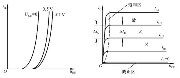
Concept and application of 0.4
feedback circuitFeedback is a process in which part or all of the output (current or voltage) of the amplifier circuit is applied to the input loop in a certain way through a certain form of feedback sampling network in an electronic system to influence the input of the amplifier circuit.
The types of feedback are: voltage series negative feedback, current series negative feedback, voltage parallel negative feedback and current parallel negative feedback.
There are four influences on the performance of negative feedback amplifier:
Improve the stability of amplification factor. Due to the change of external conditions (T℃, Vcc, device aging, etc.), the amplification factor will change. The smaller the relative change, the higher the stability.
Reduce nonlinear distortion and noise.
The input resistance Ri and output resistance Ro of the amplifier are changed.
Effectively extend the passband of the amplifier.
Characteristics of negative voltage feedback: the output voltage of the circuit tends to remain constant.
Characteristics of current negative feedback: the output current of the circuit tends to remain constant.
The general principles of introducing negative feedback are:
In order to stabilize the static working point of the amplifier circuit, DC negative feedback should be introduced; In order to improve the dynamic performance of the amplifier circuit, AC negative feedback (polarity in the middle frequency band) should be introduced.When the internal resistance of signal source is small or the input resistance of amplifier circuit needs to be increased, series negative feedback should be introduced;
When the internal resistance of the signal source is large or the input resistance is required to be reduced, feedback should be introduced and contacted.
According to the requirements of the load on the output power or output resistance of the amplifier circuit, it is decided whether to introduce voltage or current negative feedback. If the load requires stable signal voltage or small output resistance, voltage negative feedback should be introduced. If the load requires a stable signal current or the output resistance is large, the current negative feedback should be introduced.
When signal conversion is needed, the appropriate configuration should be selected according to the functions of four types of negative feedback amplifier circuits. For example, when the current-voltage signal conversion is required, the voltage parallel negative feedback should be introduced into the amplifier circuit.
Passive filter: This circuit mainly consists of passive components R, L and C.
Active filter: it is composed of integrated operational amplifier and R and C, and has the advantages of no inductance, small size and light weight.
The open-loop voltage gain and input impedance of the integrated operational amplifier are very high, and the output resistance is small. After forming an active filter circuit, the integrated operational amplifier also has a certain voltage amplification and buffering function.
However, the bandwidth of the integrated operational amplifier is limited, so it is difficult for the current active filter circuit to work at a high frequency.
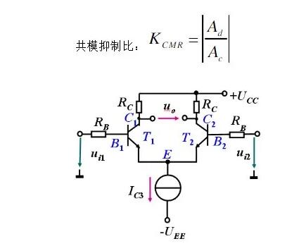
Two pairs of signals with equal size and opposite polarity are called differential mode signals. When differential amplifier circuit inputs differential mode signals (uil =-ui2), it is called differential mode input.
Two pairs of signals with equal size and same polarity are called common-mode signals. When the differential amplifier circuit inputs the common-mode signal (uil =ui2), it is called common-mode input.
In the differential amplifier, the useful signal is input in differential mode and the interference signal is input in common mode, so the interference signal will be suppressed very little.
When the environmental conditions change greatly, it is more appropriate to use FET.
FET is often used as a preamplifier to improve the input impedance of instruments and equipment and reduce noise.
The amplification capability of FET is lower than that of transistor.
Simple process, small chip area, and suitable for large scale integrated circuits. It is widely used in pulse digital circuits.
The emitter junction is forward biased and the collector junction is reverse biased.
The input circuit should be connected so that the input signal can be loaded to the input of the amplifier without loss.
The output circuit should be connected so that the output signal can be transmitted to the load as much as possible.
The transistor must be biased in the amplification region. The emitter junction is forward biased and the collector junction is reverse biased.
Set the correct static working point so that the whole waveform is in the amplification area.
The input circuit converts the changed voltage into the changed base current.
The output circuit converts the changing collector current into the changing collector voltage, and only outputs the AC signal after capacitor filtering.
The output power is as large as possible.
high efficiency
Small non-linear distortion
Heat dissipation and protection of transistor
The so-called frequency compensation refers to increasing or decreasing the strength of a signal with a specific frequency, which is used to make up for the weakening or strengthening of the frequency in the signal processing process. There are commonly used negative feedback compensation, emitter capacitance compensation, inductance compensation, etc.
The purpose of frequency compensation in the amplifier circuit is twofold: first, to improve the high-frequency characteristics of the amplifier circuit; The second is to overcome the self-excited oscillation phenomenon caused by negative feedback, so that the amplifier can work stably.In the amplifier circuit, the high frequency band of the frequency response of the amplifier circuit is often unsatisfactory due to the existence of transistor junction capacitance. To solve this problem, the common method is to introduce negative feedback into the circuit.Then, the introduction of negative feedback introduces a new problem, that is, the negative feedback circuit will appear self-excited oscillation phenomenon, so in order to make the amplifier circuit work normally and stably, it is necessary to compensate the frequency of the amplifier circuit.The frequency compensation methods can be divided into advance compensation and lag compensation, which mainly change the phase-frequency characteristics of the open-loop gain of the amplifier circuit in high frequency band by connecting some resistance-capacitance elements. At present, the most widely used phase-locked loop is.
Function of Amplifier: Amplifier circuit is one of the widely used circuits in electronic technology. Its function is to amplify the weak input signals (voltage, current and power) to the value required by the load without distortion.
Amplification circuit type:Voltage amplifier: the input signal is very small, so it is required to obtain a large output voltage without distortion, also called
small signal amplifier;Power amplifier: the input signal is large, which requires the amplifier to output enough power, also called large signal amplifier.
Difference channel is a circuit with such a function that the input of the circuit is the input of two signals, and the difference between these two signals is the effective input signal of the circuit, and the output of the circuit is the amplification of the difference between these two input signals.
Imagine such a scenario, if there is an interference signal, the two input signals will have the same interference, and the effective input of the interference signal will be zero through the difference between them, thus achieving the purpose of anti-common mode interference.
Phase locking: Lock the phase and frequency at a fixed value.
Phase-locked loop: A loop that locks the phase.The PLL consists of phase detector PD+frequency divider+loop filter LPF+voltage controlled oscillator VCO, etc.
Working principle of PLL:
The output of voltage controlled oscillator is collected and divided;
And simultaneously inputting the reference signal and the reference signal into the phase detector;
The phase detector compares the frequency difference of the two signals, and then outputs a DC pulse voltage;
Controlling the VCO to change its frequency;
In this way, after a short time, the output of VCO will be stable at a certain expected value.
Reference signal:

The phase detector is a phase comparison circuit. The input reference signal is compared with the output signal of VCO, and an error signal representing the phase difference is output. Through the loop filter, the harmonic and clutter components in the error signal are filtered out, and the error voltage is obtained to control the VCO, so that the frequency of the voltage-controlled oscillator changes in the direction of reducing the frequency difference and phase difference between the two signals, and finally the output signal frequency of VCO is equal to the frequency of the reference signal.
Zero drift means that when the input of the amplifier circuit is short-circuited, there is a slowly changing voltage at the output, that is, the output voltage deviates from the original starting point and drifts up and down.
The methods to suppress zero drift generally include:
Adopt constant temperature measures;
Compensation method, using thermosensitive element to offset the change of amplifier tube or using amplifier tube with the same characteristics to form differential amplifier circuit;
Adopt DC negative feedback to stabilize the static working point;
Resistor-capacitance coupling or specially designed modulation and demodulation DC amplifier is adopted between the stages.
Frequency response: usually also called frequency characteristic. Frequency response or frequency characteristic is a technical index to measure the adaptability of amplifier circuit to different frequency input signals.
In the amplifier circuit, due to the existence of reactive elements (such as capacitors, inductors, etc.) and the inter-electrode capacitance of transistors, when the frequency of the input signal is too low or too high, the value of the amplification factor of the amplifier circuit will be reduced, and the phase lead or lag will also occur.
That is to say, the amplification factor (or gain) of the amplifier circuit is a functional relationship with the frequency of the input signal, and we call this functional relationship the frequency response or frequency characteristics of the amplifier circuit.
In essence, frequency response refers to the relationship between the gain and frequency of an amplifier. Generally speaking, a good amplifier should not only have sufficient amplification, but also have good fidelity.
That is, the nonlinear distortion of the amplifier should be small, and the frequency response of the amplifier should be good. "Good" means that the amplifier should amplify signals with different frequencies equally.
The reasons of frequency response are as follows: First, the actual amplified signal frequency is not single; Second, the amplifier has reactive elements and reactive factors.Due to the existence of reactive components in the amplifier circuit (such as the inter-electrode capacitance of the tube, the load capacitance, the distributed capacitance, the coupling capacitance, the emitter bypass capacitance, etc.), the amplifier may have different amplification factor and phase shift for different frequency signal components.If the amplification circuit amplifies the amplitude of signals with different frequencies differently, it will cause amplitude distortion; If the amplification circuit produces different phase shifts to different frequency signals, it will cause phase distortion.Amplitude distortion and phase distortion are always called frequency distortion. Because this distortion is caused by the linear reactive components (resistors, capacitors, inductors, etc.) of the circuit, it is not called linear distortion. In order to amplify the signal without distortion, it is necessary to study the frequency response of the amplifier.The frequency response of the amplifier circuit can be described by amplitude-frequency characteristic curve and phase-frequency characteristic curve, if the amplitude-frequency characteristic curve of an amplifier circuit is a straight line parallel to the X axis (or parallel to the X axis in the frequency range of interest).The frequency response is stable when the phase-frequency characteristic curve is a straight line passing through the origin or a straight line passing through the origin in the concerned frequency range.
The methods of changing frequency response mainly include:
Change the component parameters of the amplifier circuit;
Introducing new components to improve the frequency response of the existing amplifier circuit;
A new amplifier circuit is connected in series with the original amplifier circuit to form a multistage amplifier circuit.

The received signal is strong and weak, and there is a big disparity. If AGC is not added, the output will fluctuate greatly, which will affect the effect.
In order to receive weak signals, the amplifier of the receiver is always large, that is, it has high sensitivity. However, when receiving strong signals, if the amplifier of the channel is not regulated, it will have adverse consequences.
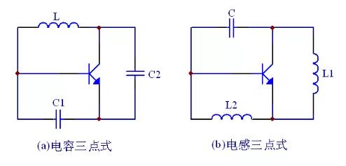
Inductive three-point oscillator and capacitive three-point oscillator.
With the increase of operating frequency, the amplifier will produce additional phase shift, which may turn negative feedback into positive feedback and cause self-excitation. High frequency self-excitation can be eliminated by phase compensation.
The principle of phase compensation is: in the middle stage with high amplification, a small capacitor C (tens to hundreds of picofarads) is used to form a voltage parallel negative feedback circuit, and the phase-frequency characteristics and amplitude-frequency characteristics can be modified by capacitor correction and RC correction respectively.
Let the common-mode component be Yc, and the differential-mode component be Yd, then the output is:
Y+=Yc+Yd
Y-=Yc-Yd
In the amplifier circuit, it is usually expected that the input resistance of the amplifier circuit is high, because it has little influence on the signal source.
Seen from the output of the amplifier circuit, the amplifier circuit can be equivalent to a signal source with a certain internal resistance, and the internal resistance of the signal source is the output resistance. Usually, it is hoped that the smaller the value, the better, because this can improve the load capacity of the amplifier.
Function:
Change the AC voltage into a stable DC voltage with appropriate size.

Power transformer: changing AC grid voltage u1 into appropriate AC voltage u2.
Rectifying circuit: changing AC voltage u2 into pulsating DC voltage u3.
Filter circuit: converts pulsating DC voltage u3 into smooth DC voltage u4.
Voltage stabilizing circuit:
Eliminate the influence of power grid fluctuation and load change, and keep the output voltage uo stable.
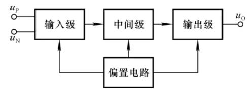
Bias circuit:Set appropriate static working points for amplifier circuits at all levels, and often use constant current source circuits.
Input stage: it is usually a differential amplifier circuit, which requires large Ri, large Ad and small Ac, and the input terminal has high withstand voltage. It has in-phase and anti-phase input terminals.
Intermediate stage: the main amplifier stage is usually a common-emitter amplifier circuit, which mostly adopts composite tubes, and requires sufficient amplification capability.
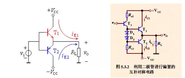
Output stage: power stage, which mostly adopts complementary power amplifier circuit or emitter output device. It is required that Ro is small, maximum distortion is avoided, and the output voltage is as large as possible.
First-order active low-pass filter and first-order active high-pass filter.

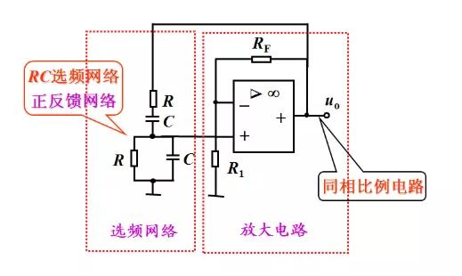
Composition of sine wave oscillation circuit:
Amplification circuit: amplifying signal
Feedback network:
it must be positive feedback, and the feedback signal is the input signal of the amplifier circuit.
Frequency selection network: ensure that the output is a sine wave with a single frequency, even if the circuit only meets its own oscillation conditions at a specific frequency.
Amplitude stabilization link: enables the circuit to switch from ½ AuF½ > 1, transition to ½ AuF½ =1, thus achieving stable amplitude oscillation.
Disclaimer: This article is reproduced from "Hardware Attacking the City Lion". This article only represents the author's personal views, and does not represent the views of Sacco Micro and the industry. It is only for reprinting and sharing to support the protection of intellectual property rights. Please indicate the original source and author when reprinting. If there is any infringement, please contact us to delete it.
Company Tel: +86-0755-83044319
Fax/fax:+86-0755-83975897
Email: 1615456225@qq.com
QQ: 3518641314 Manager Li
QQ: 332496225 Manager Qiu
Address: Room 809, Block C, Zhantao Technology Building, No.1079 Minzhi Avenue, Longhua New District, Shenzhen



Site Map | 萨科微 | 金航标 | Slkor | Kinghelm
RU | FR | DE | IT | ES | PT | JA | KO | AR | TR | TH | MS | VI | MG | FA | ZH-TW | HR | BG | SD| GD | SN | SM | PS | LB | KY | KU | HAW | CO | AM | UZ | TG | SU | ST | ML | KK | NY | ZU | YO | TE | TA | SO| PA| NE | MN | MI | LA | LO | KM | KN
| JW | IG | HMN | HA | EO | CEB | BS | BN | UR | HT | KA | EU | AZ | HY | YI |MK | IS | BE | CY | GA | SW | SV | AF | FA | TR | TH | MT | HU | GL | ET | NL | DA | CS | FI | EL | HI | NO | PL | RO | CA | TL | IW | LV | ID | LT | SR | SQ | SL | UK
Copyright ©2015-2025 Shenzhen Slkor Micro Semicon Co., Ltd