Service hotline
+86 0755-83044319
release time:2022-03-17Author source:SlkorBrowse:9787
The first two issues talked about RCD circuit, and inevitably mentioned the peak of switch. From this, I thought of our most commonly used circuit, Buck circuit.
Buck oscillation waveform
The SW waveform in front of the inductance of Buck circuit must have been measured by everyone. Generally speaking, it is nothing more than the following two kinds:
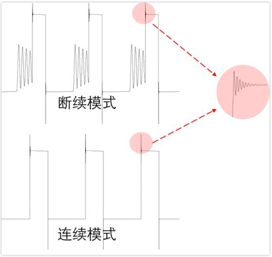
Whether it is continuous mode or intermittent mode, there will be a rising peak or a falling peak, which is just a matter of size.
If we look at it, the peak can be seen as an oscillating waveform with a high frequency.
Or, more obviously, in intermittent mode, when the inductance current decreases to 0, it starts to oscillate, with a large amplitude and a low frequency.
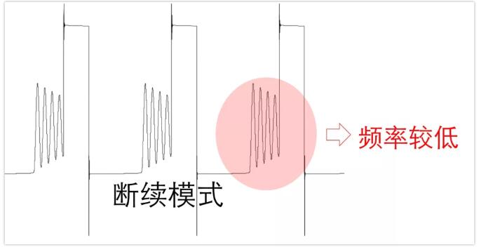
For novices, they may be drumming in their hearts: Is there something wrong with this oscillation?
The above oscillations, or spikes, need to understand why they grow like this. Is there a problem? How to suppress it? If you want to know the ins and outs in detail, it is not easy.
These waveforms, in essence, are LC damped oscillations. In this section, we will first understand the various situations of LC damped oscillations.
LC damped oscillation
The mechanism of these waveforms is that the inductor or capacitor is charged before the switch is turned off.
After the switch is turned off, the energy of the inductor or capacitor needs to be released, so the parasitic capacitance or inductance in the circuit will be found, and combined with the equivalent resistance in the circuit, LC damping oscillation is formed.
How Buck specifically constitutes LRC loop, because it involves many parasitic parameters, and this is not easy to figure out, which will be described in detail later.The theme of this section is LC damping oscillation.
Let's take the simplest LRC series circuit as an example.
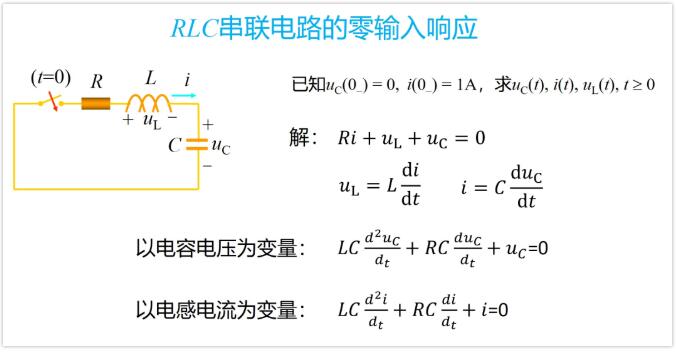
In fact, this circuit should have been studied in the university course "Circuit Analysis" (like the course "Signals and Systems"), and it is a second-order circuit.If you want to look at the theoretical analysis again, you can look at the following link:
https://wenku.baidu.com/view/6c61d292a26925c52dc5bfc8.html
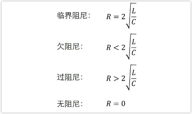
The waveform of this circuit can be divided into four situations, namely:
Get a new skill recently, and try to use LTspice simulation. It feels good, more convenient than Matlab. Of course, it can only show that the emphasis of the two softwares is different. Matlab is a mathematical tool. If the following results can be obtained with Matlab, the understanding will certainly be deeper, but it will be more difficult.
Let's take a look at my LTspice simulation:
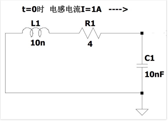
Initial conditions: L=10nH C=10nF Initial inductor current I=1A, capacitor voltage is 0V.
According to formula 2 (l/c) 0.5, the critical damping resistance r = 2ω is obtained.
Let's just change the resistance R so that R=4Ω, 2Ω, 1Ω, 0.1Ω, 0Ω. Let's look at the waveforms respectively:
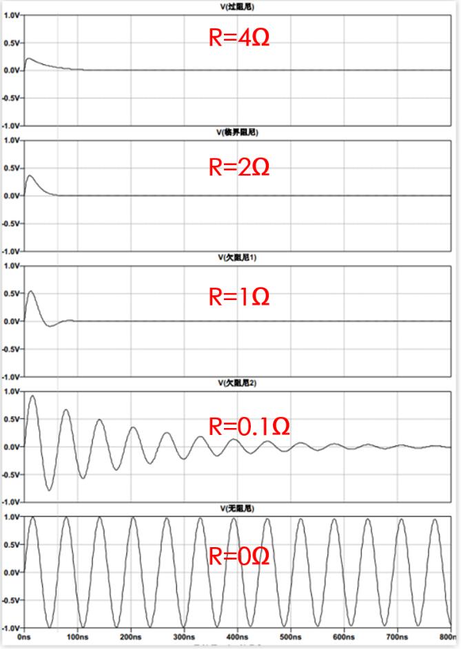
We can get the oscillation frequency from the above figure:
Comparing the waveforms of R=0.1 and R=0, we can see that the period of oscillation (the time difference between two peaks) is the same, which is about 62.8ns In fact, this is equal to the resonant frequency of LC circuit.
What's the use of knowing this frequency?
We can get the total inductance or capacitance of the circuit according to this.In practice, we can usually measure the frequency of the oscillation peak with an oscilloscope, and then we can artificially connect a capacitor.
At this time, the peak frequency will definitely change, and then we can measure it with an oscilloscope.According to the frequency before and after, and the increased capacitance, we can calculate how big the parasitic capacitance and inductance are.
The following is the snuber circuit explained in a document (BUCK circuit is often used for peak removal)
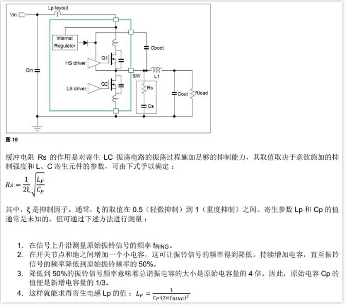
Now you should know the basic principle of this method.
Disclaimer: This article is reproduced from "Notes of Electronic Engineers". This article only represents the author's personal views, and does not represent the views of Sacco Micro and the industry. It is only for reprinting and sharing to support the protection of intellectual property rights. Please indicate the original source and author when reprinting. If there is any infringement, please contact us to delete it.
Company Tel: +86-0755-83044319
Fax/fax:+86-0755-83975897
Email: 1615456225@qq.com
QQ: 3518641314 Manager Li
QQ: 332496225 Manager Qiu
Address: Room 809, Block C, Zhantao Technology Building, No.1079 Minzhi Avenue, Longhua New District, Shenzhen



Site Map | 萨科微 | 金航标 | Slkor | Kinghelm
RU | FR | DE | IT | ES | PT | JA | KO | AR | TR | TH | MS | VI | MG | FA | ZH-TW | HR | BG | SD| GD | SN | SM | PS | LB | KY | KU | HAW | CO | AM | UZ | TG | SU | ST | ML | KK | NY | ZU | YO | TE | TA | SO| PA| NE | MN | MI | LA | LO | KM | KN
| JW | IG | HMN | HA | EO | CEB | BS | BN | UR | HT | KA | EU | AZ | HY | YI |MK | IS | BE | CY | GA | SW | SV | AF | FA | TR | TH | MT | HU | GL | ET | NL | DA | CS | FI | EL | HI | NO | PL | RO | CA | TL | IW | LV | ID | LT | SR | SQ | SL | UK
Copyright ©2015-2025 Shenzhen Slkor Micro Semicon Co., Ltd