Service hotline
+86 0755-83044319

release time:2022-03-17Author source:SlkorBrowse:11885
Fund project:Shenzhen Science and Technology Commission Project(JCYJ20180508161601937)
1
Power electronic devices are developing towards high frequency, high density, high power and high temperature applications [1]. At present, silicon (Si)-based devices still dominate. However, due to the characteristics of materials, the switching frequency, operating temperature and power density of silicon-based devices are limited. Compared with traditional silicon-based devices, the third-generation semiconductors such as silicon carbide (SiC) and gallium nitride (GaN) are more and more used in high-voltage, high-temperature and high-frequency applications such as wireless communication, electric vehicles and aerospace because of their higher breakdown voltage, wider band gap, higher thermal conductivity and lower power loss [2-3]. At the same time, however, the rapid development of the third generation semiconductor devices has put forward more stringent requirements for packaging technology.
Packaging technology is a process of connecting and fixing the chip with the carrier substrate, leading out the pins, and molding them into a whole power device or module, which mainly plays the role of electrical connection, structural support and protection, and providing heat dissipation [4]. As the core of module integration, packaging materials, processes and structures directly affect the thermal, electrical and electromagnetic interference characteristics of power modules. At present, the mature packaging technology is mainly based on connecting materials such as silver glue or tin-based solder, and packaging structures such as lead connection, which have poor high-temperature and high-pressure resistance, prominent electromagnetic compatibility problems, and cannot provide an efficient heat dissipation way. Recently, sintered silver interconnect materials, three-dimensional integrated package structures, etc. have excellent high temperature resistance and high thermal conductivity, which can achieve double-sided heat dissipation and greatly reduce switching losses, making power modules have good thermal and electrical characteristics and reliability, and have gained more and more research and attention. It is expected to meet the reliable application of the third generation semiconductor devices in the fields of high temperature, high voltage and high frequency. In this paper, the latest research progress of power electronic packaging materials and structure design is summarized and prospected.
2
A typical power module package structure is shown in Figure 1, which consists of a power chip, connecting materials, bonding wires, ceramic substrate, bottom plate, potting materials, shell and power terminals [3,5]. The thermal, electrical, mechanical and chemical properties of each packaging material are different, so it is necessary to comprehensively consider the properties of each material to select the best performance of the whole power module.
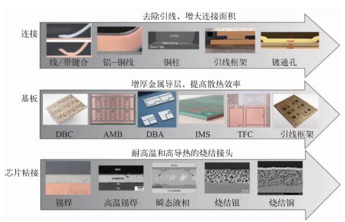
图1 典型的功率模块封装结构[5]
The development trend of key packaging materials and technologies such as chip bonding, connection and substrate is shown in Figure 2. The technology of connection is developing from bonding wires to ribbons, copper pillars, lead frames and plated through holes, etc. By removing leads and increasing the connection area, the thermal and electrical conductivity is improved. The bonding materials for chips have developed from traditional soldering to gold-based high-temperature soldering, transient liquid-phase bonding, sintered silver and sintered copper, etc., which greatly improve the thermal and electrical conductivity and meet the high-temperature and reliable applications. The substrate develops towards thickening the metal conductive and thermal conductive layer of ceramic substrate, thus improving the heat dissipation efficiency [5].
Figure 2 Development trends of packaging materials and technologies such as connection, substrate and chip bonding [5]
The performance parameters of commonly used semiconductor materials are shown in Table 1 [6-7]. Because of its mature technology and low cost, Si is widely used in various discrete devices and integrated circuits, electronic information network engineering and other fields. Compared with Si, GaAs has the characteristics of wide band gap and high electron mobility, which can significantly reduce RF size and power consumption, and is widely used in low-power devices in RF, wireless communication and optoelectronic fields. SiC and GaN have larger band gap, are not easy to absorb thermal radiation energy and jump to conduction band when working at high temperature, and have higher breakdown field strength, so wide band gap semiconductors SiC and GaN are more suitable for high temperature and high voltage occasions than Si. SiC has higher thermal conductivity, better heat dissipation capacity, higher carrier mobility, higher current density, and high temperature and high voltage resistance, so it is often used as a power device, which has obvious advantages in the high power field with voltage of 600 V and above, and is widely used in the fields of new energy vehicles and power equipment. GaN has faster electron mobility and carrier velocity, smaller on-resistance and parasitic parameters at high voltage, and has obvious advantages in the direction of high power radio frequency. GaN is mainly used in microwave RF fields such as 5G communication and satellite communication, power electronics fields such as fast charging of consumer electronics and new energy vehicles, and LED optoelectronics fields because of its high power density, low energy consumption, high frequency and wider bandwidth. Similar to SiC, GaN technology is still in the rapid development stage at present, and the cost is relatively high.
Table 1 Properties of Semiconductor Chip Materials [6]
SnPb alloy solder, such as Sn63Pb37, has been widely used in chip bonding materials because of its excellent properties, such as low shear modulus, high wettability, ductility, thermo-mechanical properties and reliability. However, SnPb doesn't meet the EU RoHS lead-free standard, and its melting point is low (about 180℃). Therefore, new chip bonding materials are needed to meet the requirements of thermal expansion coefficient (CTE) matching and high temperature resistance of packaging structures and materials.At present, the most widely used chip bonding materials are shown in Table 2 [8]. Conductive silver paste is mainly composed of resin matrix, conductive particles (mainly silver powder), dispersing additives and additives, etc. Its electrical conductivity and thermal conductivity are relatively low, and its glass transition temperature is about 100~150℃, which is limited in the field of high-temperature and high-pressure chip packaging. Compared with SnPb solders, lead-free solders, such as SnAg or SnAgCu, generally have a higher Sn content than 90% and a higher melting point (about 220℃). In the solidification process, the undercooling degree is higher, and it is easy to form coarse dendritic structures and intermetallic compounds, which are unevenly distributed, thus weakening its creep resistance. In addition, SnAgCu alloy has a high elastic modulus, and its CTE is quite different from that of chip and substrate. Under the action of thermal cycle load, it is easy to cause fatigue damage and lead to solder joint peeling, which reduces the reliability of solder joint [9].
Table 2 Properties of die bonding materials [8]
High-temperature bonding materials for chips, such as gold-based eutectic alloy solders such as AuSn or AuGe, have high melting point (greater than 280℃), thermal conductivity and electrical conductivity, and are easy to realize solderless brazing. However, the gold content in gold-based solders is generally high and the cost is high, and because of the high brittleness of the component phase, it leads to the disadvantages of difficult processing, low yield and poor product performance, which seriously affects its wide application in the field of power electronic packaging [10].
Transient liquid phase bondIng (TLPB) is a process in which intermediate layers (such as In and Sn) with lower melting points are added to the joined base materials (such as Cu, Au, Ag and Ni) with higher melting points, and the intermediate layers and some base materials are melted and re-solidified by heating, so that solid and liquid diffuse each other to form a connection. Choosing suitable materials and processes, transient liquid-phase bonding can form joints with excellent performance, such as bonding strength greater than 60 MPa[11]. However, the application of transient liquid-phase connection in high-temperature chip interconnection is greatly limited due to the low choice of intermediate layer, high cost and the oxidation of Au-In and other materials.
Sintered silver interconnection, also known as low-temperature connection technology, is based on solid-phase atom diffusion of nano-silver or micro-silver particles to form sintered connection. Because of its low sintering temperature (200~300℃) and high melting point (961℃), silver has many advantages, such as high thermal conductivity, resistance to temperature cycling and high reliability of power cycling. It has become the preferred choice for high-temperature chip interconnection, and has been widely studied and applied [12]. However, sintering silver also has some disadvantages, such as high cost, low-temperature agglomeration of nano-silver particles, pressure sintering of micron silver solder paste, complicated process, Ni/Au or Ni/Ag plating on the surface of chip and substrate, and electrochemical migration of silver. Compared with nano-silver solder paste, nano-copper solder paste has attracted attention recently because of its lower cost and no reliability risk of electrochemical migration [13]. However, nano-copper particles are easily oxidized and need to be sintered in inert atmosphere, which increases the process complexity and equipment cost, and has certain application limitations.
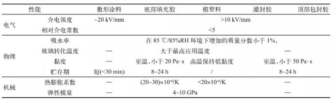
The main function of plastic packaging material is electrical insulation and environmental isolation, which plays the protective role of moisture-proof, salt spray-proof, mildew-proof, dust-proof, collision-proof and vibration-proof, avoiding environmental corrosion and damage, thus ensuring the electrical performance of electronic components, even improving the voltage level of high-voltage power modules, avoiding electrode discharge, and finally improving the reliability of electronic products [14]. The types and properties of plastic packaging materials are shown in Table 3. Plastic packaging materials can be divided into Conformal Coatings, Underfills, Molding Compounds, Potting Compounds and globtops [14].
Table 3 Types and properties of plastic packaging materials [14]
Conformal coating is a kind of organic coating commonly used for surface protection of printed circuit, which needs good connection performance with substrate and components. Generally, materials with low water absorption, high dielectric strength, matched CTE and low elastic modulus are selected, such as acrylic acid which can be used at low temperature less than 120℃, polyurethane which can be used at low temperature less than 165℃, epoxy resin which can be used at medium temperature less than 200℃, and silicone resin, parylene, benzocyclobutene and polyimide which can be used at high temperature greater than 250℃.
As shown in Figure 3, underfill and molding compound can not only isolate from the surrounding environment and reduce the electric field stress, but also improve the reliability of packaged products by reducing or redistributing the thermo-mechanical stress caused by CTE mismatch [14]. Therefore, materials matching the CTE of each component in the package structure should be selected as much as possible, such as hard materials with CTE of (20~30)×10-6/K and less than 20×10-6/K as underfill and molding compound, respectively, to reduce the thermal stress from solder balls and the whole package structure including solder balls. At present, the most commonly used underfill and molding compound is epoxy resin filled with silica.
The potting glue and the top encapsulating glue not only improve the voltage level against electric field breakdown and avoid the corrosion and damage of the surrounding environment, but also play a certain role in mechanical support of the packaging structure. At present, the most commonly used potting glue and top sealing glue materials are polyurethane which can be applied at a low temperature of less than 165℃, epoxy resin which can be applied at a medium temperature of less than 200℃, and silicone rubber or gel which can be applied at a high temperature of less than 300℃. Among them, soft materials such as silicone rubber or gel are widely used because of their low hardness and modulus, high plasticity and elasticity, which have little influence on the stress of packaging components such as chips and bonding wires. However, soft materials such as silicone rubber and gel have poor mechanical support and protection performance. In order to resist external impact, hard materials such as resin can be selected. However, resin usually has a high modulus, so it is necessary to choose materials with matching CTE to avoid excessive thermo-mechanical stress on the whole package structure.
(b)模塑料示意图
Figure 3 Schematic diagram of underfill and molding compound in power electronic packaging structure [14]
Generally speaking, the substrate is a sandwich structure of "metal conductive layer-insulation layer-metal conductive layer", and the upper and lower metal conductive layers are used for the interconnection of the chip and the backplane respectively. According to the manufacturing process, the substrates can be divided into Direct Bonded Copper substrate (DBC), Direct Printed Copper substrate (DPC), Direct Bonded Aluminum substrate (DBA), Active Metal Brazing substrate, AMB), Insulated Metal Substrate (IMS) and Thick-film Printed Copper (TPC), etc.
DBC substrate is a eutectic connection between ceramic and thin copper oxide on copper film, which has excellent performance and relatively low cost, and is widely used in power electronic packaging. However, the copper oxide film at the ceramic interface is easy to delaminate, resulting in low reliability of DBC substrate against temperature cycling. AMB substrate connects metal and ceramic together by active metal brazing, which can eliminate oxide layer and improve reliability. DBA uses AlSi brazing to connect aluminum plate and ceramics. Compared with DBC's copper layer, the aluminum layer has lower hardness, can withstand higher thermal-mechanical stress and improve reliability [15]. However, the thermal conductivity of aluminum is lower than that of copper, and the heat dissipation performance of DBA substrate is not as good as DBC substrate. IMS substrate includes a layer of insulating resin with high thermal conductivity, a copper bottom plate and a thick copper film. Compared with DBC, IMB has the advantages of simple manufacturing process, low heat treatment temperature, low cost and high reliability. TPC is a layer of copper paste printed on ceramic by screen printing, which is sintered at 850~950℃ to form a high-strength connection between metal film and ceramic. The temperature cycle reliability is high, and it can be highly integrated with integrated circuit chips and passive devices to form a hybrid module. Recently, the substrate based on thick lead frame and thin insulation layer also appeared, which simplified the structure of multilayer substrate and improved the heat dissipation efficiency [5].
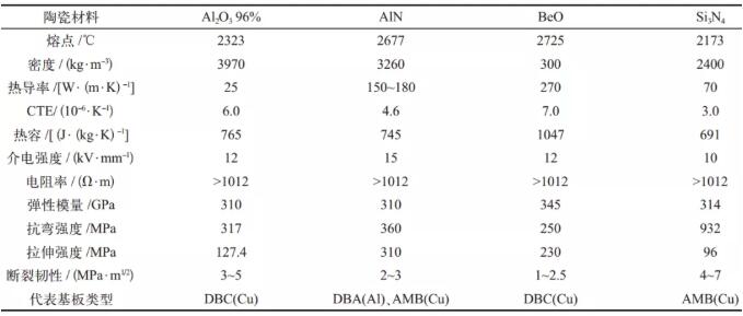
Considering the thermal conductivity and CTE, Al2O3, Si3N4, AlN and BeO are the most commonly used ceramic materials in the substrate. See Table 4[8,16] for their performance comparison. BeO has the highest thermal conductivity, but the dust in the preparation process is harmful to human body, which limits its application. Al2O3 is the most economical choice, but its mechanical strength is moderate and its thermal conductivity is relatively poor. The thermal conductivity of AlN is higher than that of Al2O3, and the CTE is better matched with the chip. Si3N4 has higher temperature cycling reliability, but its cost is relatively high [17]. Relatively speaking, the combination reliability of Al-AlN and Cu-Si3N4 is higher, because the former aluminum material is soft, its elastic modulus is low, and it is easy to deform, which can slow down the damage caused by thermal stress to ceramics. The latter Si3N4 has higher bending strength and fracture toughness, and can resist the thermal stress caused by copper.
Table 4 Properties of Ceramic Materials in Substrates [8]
The most commonly used base plate material is Cu. In order to reduce CTE and ensure high thermal conductivity, metal composite materials such as AlSiC, W-Cu, Mo-Cu and Cu-Mo-Cu are also widely used. See Table 5[8] for their performance parameters. Generally, the base plate will be plated with nickel, which can prevent the migration and oxidation of copper atoms at high temperature and improve the strength and deformation resistance of the copper base plate.
Table 5 Material Properties of Bottom Plate [8]
3
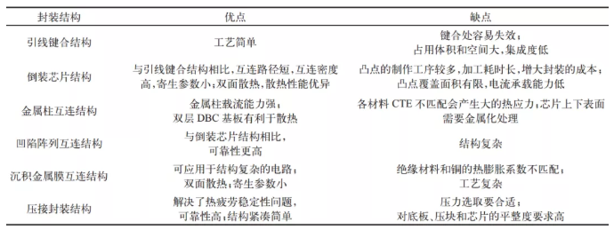
According to different chip assembly methods and interconnection processes, power electronic packaging structures can be divided into two types: soldering packaging and crimping packaging. The development trend of the package is shown in Figure 4, in which the soldered package can adopt wire bonding, flip chip (BGA interconnection), metal pillar interconnection, recessed array interconnection, deposited metal film interconnection and other structures. Press-on packaging is an interconnection structure formed by external mechanical pressure. For the convenience of comparative analysis, the advantages and disadvantages of the above packaging methods are listed in Table 6[18]. Wire bonding has the advantages of mature technology, low cost and flexible wiring. However, wire-bonded modules have high parasitic inductance, which can only dissipate heat from one side of the backplane [18]. Moreover, due to the mismatch of CTE between the bonding wire and the chip, large thermo-mechanical stress is generated, which makes the solder joints prone to fatigue failure, and becomes the main failure form of the module in the process of power cycle.
Figure 4 Development trend of package structure [5]
Table 6 Comparison of package structures [18]
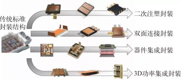
At present, the power electronic packaging structure has gradually developed from the traditional wire bonding standard packaging structure to Overmold, Double-Side Bonding, Component Integration and 3D Power Integration. By removing leads, electromagnetic interference can be reduced, heat dissipation efficiency can be improved, and integration can be increased. Among them, the injection molding structure is a compact planar package, which is easy for batch module production; Double-sided connection structure can realize double-sided heat dissipation and improve heat dissipation efficiency; The integrated structure of the device can integrate various functions in the module, and improve the switching speed; Three-dimensional power integration structure is to stack chips in the vertical direction, which can greatly reduce parasitic inductance and improve switching performance [5]. Compared with two-dimensional packaging, three-dimensional packaging has obvious advantages, such as greatly shortening the loop distance in the vertical direction, reducing parasitic inductance and electromagnetic interference, increasing transmission speed, improving switching performance and reducing power loss; It can integrate a variety of chips and devices, such as gate drive circuits, decoupling capacitors, heat sinks, etc., to further improve the power integration density and reduce the package volume. However, at present, 3D packaging also faces some challenges, such as thermal management, production technology and yield caused by chip stack interconnection, and the manufacturing process needs to be further improved [6,19].
On the basis of the traditional wire bonding packaging structure, the two-shot packaging structure is a structure in which the chip is directly bonded to the lead frame, the bonding wires are removed, and the epoxy resin is used for injection packaging. Compared with the package structure of wire bonding, the connection area at the top of the chip in injection molding package increases, which improves the heat dissipation efficiency. The reduction of parasitic inductance reduces the power loss, which is very beneficial to modular mass production and is widely used in rectifiers of electric vehicles.
The double-sided connection structure connects the chip with the upper and lower substrates respectively, such as the SKiN power module [20] proposed by Ximenkang Company and the SiC power module [21] proposed by Fuji Electric, which can achieve the purpose of removing bonding wires. The double-sided connection package structure has two main advantages: (1) eliminating the wire bonding on the emitter surface, effectively reducing parasitic inductance, voltage overshoot and power loss, and improving switching performance; (2) Realize the heat dissipation of the chip in the upper and lower directions, improve the heat dissipation efficiency, and effectively reduce the junction temperature of the chip, thus slowing down the failure. Oak Ridge National Laboratory proposed a Si IGBT or SiC MOSFET power module with double-sided DBC substrate package. Compared with the traditional wire bonding module, its inductance decreased by 62%, switching loss decreased by 50%~90%, and heat dissipation efficiency increased by 40%~50%[22].
However, the double-sided connection structure also has some disadvantages. Firstly, compared with the wire bonding module, the double-sided connection structure has more layers of materials, which increases the complexity of the packaging process. Secondly, because the CTE of each layer of materials is different, thermal mismatch will produce greater thermal-mechanical stress, which will reduce the reliability of the connecting layer. In order to reduce the thermo-mechanical stress, some metals matching the CTE of the chip, such as Mo or Cu/Mo/Cu[23], are used as the interlayer materials. Thirdly, as shown in Figure 5, when realizing a power module with multi-chip double-sided connection with different thicknesses, it is necessary to electroplate or connect Micro-Metal Post or copper pins with different heights between the chip and DBC substrate, so as to solve the height difference problem caused by different thicknesses of multi-chips [6]. Fourthly, tin-based solder is the most commonly used interconnection material in module packaging. In the process of double-sided connection module packaging, it usually needs multiple connection steps, which requires a group of solders with different melting points, which limits the service temperature of the module. Therefore, in the double-sided connection package structure, the sintered silver solder paste with high thermal conductivity, high electrical conductivity and high melting point has become the preferred choice for interconnection materials.
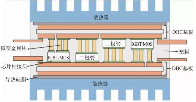
Figure 5 Double-sided connection package structure [6]
Integrated package is a device that integrates multiple functions in a module, such as integrated gate drive circuit, decoupling capacitor, temperature sensor, current sensor and protection circuit [18]. Integrated device packaging has many advantages, for example, by integrating gate drive circuit and decoupling capacitor, parasitic inductance of bus bar or external connector of module can be reduced, connection between power device and gate drive can be shortened, gate loop inductance can be reduced, electromagnetic interference can be suppressed, current sharing performance and switching speed can be improved. However, this package structure also has some limitations. For example, the integrated gate drive circuit is generally simple, and the overall size, current carrying capacity and switching frequency of the module are limited by each integrated device. In addition, before the devices are integrated and packaged, it is necessary to check the temperature resistance of each device, so as to avoid that the normal operation of the temperature sensitive devices will be affected because the device integration distance is too close [5].
The integrated package structure is shown in Figure 6. The three-dimensional package structure is mainly divided into stacked three-dimensional package and embedded three-dimensional package [24]. On the basis of two-dimensional package, it adopts wire bonding, flip chip, micro bump, Ball Grid Array (BGA), Through Silicon Via (TSV), PCB embedding and other process technologies to realize multi-chip stacked interconnection in the vertical direction [25
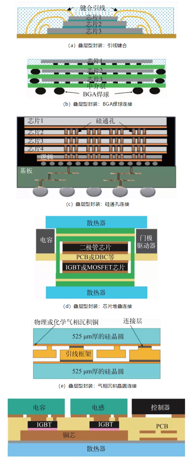
Figure 6 Schematic diagram of three-dimensional integrated package structure [6,29-31]
In the stacked 3D packaging, through-silicon vias are one of the most concerned technologies, which use the vertical interconnection of through-silicon vias through the substrate to realize the electrical interconnection between different chips [28]. The key technologies of through-silicon packaging include through-silicon hole forming, filling, chip thinning and interconnection. The concrete steps are as follows: first, through holes are formed by laser drilling, dry etching or wet etching, then SiO2 insulating layer and copper conductive layer are filled by chemical vapor deposition, then chips are thinned by grinding, and finally chips are interconnected by bonding or bonding between metals [29]. Compared with the traditional planar two-dimensional lead interconnect structure, the three-dimensional structure of silicon through hole has the advantages of small size, light weight, high efficiency of silicon wafer use, shortened signal delay and reduced power consumption, etc., and is widely used in three-dimensional wafer level, system level and integrated circuit packaging. However, it also has some limitations. Firstly, the reliability, the high power density of the through-silicon package structure, and the big thermal management problem of the laminated chip; Secondly, the cost is high, and the packaging structure, process and test are complicated.
Embedded 3D package uses copper wire and micropore instead of bonding wire, and embeds the chip in PCB laminate, which can reduce the volume, improve the reliability and facilitate system integration [30]. The biggest challenge of this structure is its poor thermo-mechanical properties, which is limited by the thermo-mechanical stress caused by the low glass transition temperature and high CTE of traditional PCB materials, and its service temperature is low [18]. In addition, the peel strength of FR4-PCB laminate is low, about 0.9 ~ 1.25 N/mm. Compared with DBC substrate, the rated power of the module embedded in PCB is low [3].
In addition to the above welding connection, three-dimensional package can also be formed by crimping. A typical case is shown in Figure 7, which is the internal structure diagram of Westcode)IGBT crimping module [32]. The components are physically connected by external mechanical pressure instead of leads, soldering or sintering. With simple structure, low cost and high reliability, it has been widely used in high-voltage and high-current power grids. However, in the crimping module, the internal dimensions of the module, the flatness and surface quality of each component are required to be high, and the thermal conductivity and electrical conductivity of the joint are greatly affected by the pressure and uniformity. It is necessary to select the appropriate clamping pressure to ensure the smaller contact resistance and thermal resistance, but it will inevitably be affected by the surface roughness and structural deformation. Elastic buffer structures and materials with small CTE, such as Mo or Be gaskets and spring plates, are often introduced into the crimping structure to equalize pressure, reduce thermo-mechanical stress and improve reliability.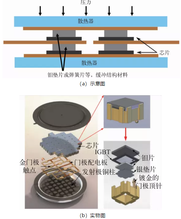
Fig. 7 Internal structure of IGBT crimping module in Sima [6,32]
4
The key materials, connection technology and structure design of power packaging are gradually developing in the direction of removing leads, improving heat dissipation performance, increasing integration density, etc., to meet the reliable application in high temperature, high voltage and high frequency environments. With the popularization and application of the third generation semiconductor devices, sintered silver solder paste connecting materials, silicon via technology, three-dimensional integrated packaging structure, etc. are the main trends in the future, and I believe their application prospects are infinite.
Disclaimer: This article is reproduced from "Electronics and Packaging". This article only represents the author's personal views, and does not represent the views of Sacco Micro and the industry. It is only for reprinting and sharing to support the protection of intellectual property rights. Please indicate the original source and author when reprinting. If there is any infringement, please contact us to delete it.


Site Map | 萨科微 | 金航标 | Slkor | Kinghelm
RU | FR | DE | IT | ES | PT | JA | KO | AR | TR | TH | MS | VI | MG | FA | ZH-TW | HR | BG | SD| GD | SN | SM | PS | LB | KY | KU | HAW | CO | AM | UZ | TG | SU | ST | ML | KK | NY | ZU | YO | TE | TA | SO| PA| NE | MN | MI | LA | LO | KM | KN
| JW | IG | HMN | HA | EO | CEB | BS | BN | UR | HT | KA | EU | AZ | HY | YI |MK | IS | BE | CY | GA | SW | SV | AF | FA | TR | TH | MT | HU | GL | ET | NL | DA | CS | FI | EL | HI | NO | PL | RO | CA | TL | IW | LV | ID | LT | SR | SQ | SL | UK
Copyright ©2015-2025 Shenzhen Slkor Micro Semicon Co., Ltd
