Service hotline
+86 0755-83044319

release time:2022-03-17Author source:SlkorBrowse:11356
MOSFET is a common voltage-type control device, which has a series of advantages such as fast switching speed, high frequency performance, high input impedance, low noise, low driving power, large dynamic range and wide safe working area (SOA). Therefore, it is widely used in switching power supply, motor control, power tools and other industries. As the weak link of MOSFET itself, if the circuit design is improper, it will easily lead to the failure of the device or even the system. Therefore, this article will sort out the common circuits of the gate for your reference and discussion, and you are welcome to put forward your own views.
Common functions of MOSFET gate circuits are as follows:
1、Remove the noise coupled into the circuit and improve the reliability of the system.
2、Accelerate the conduction of MOSFET and reduce the conduction loss.
3、Accelerate the turn-off of MOSFET and reduce the turn-off loss.
4、Lower di/dt of MOSFET, protect MOSFET DI/DT suppress EMI interference.
5、Protect the grid to prevent grid breakdown under abnormal high voltage.
6、Increasing the driving capability, MOSFET can be driven under a small signal.
The above is the function of the gate circuit that I can think of. Welcome to add your thoughts, and I will post the corresponding circuits for your discussion.The above is the function of the gate circuit that I can think of. Welcome to add your thoughts, and I will post the corresponding circuits for your discussion.
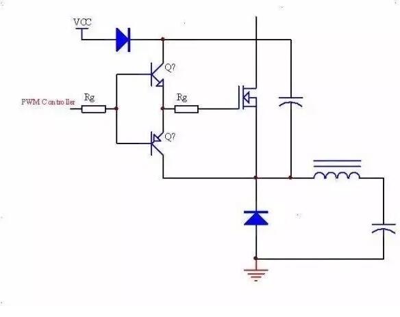
First of all, let's talk about the direct driving of power IC. The following figure is our most commonly used direct driving mode. In this kind of mode, we have not done too much processing on the driving circuit, so we should try our best to optimize the PCB LAYOUT. For example, shorten the trace length from IC to MOSFET gate, increase the trace width, and place Rg as far as possible from MOSFET gate, so as to reduce parasitic inductance and eliminate noise.
First of all, let's talk about the direct driving of power IC. The following figure is our most commonly used direct driving mode. In this kind of mode, we have not done too much processing on the driving circuit, so we should try our best to optimize the PCB LAYOUT. For example, shorten the trace length from IC to MOSFET gate, increase the trace width, and place Rg as far as possible from MOSFET gate, so as to reduce parasitic inductance and eliminate noise.
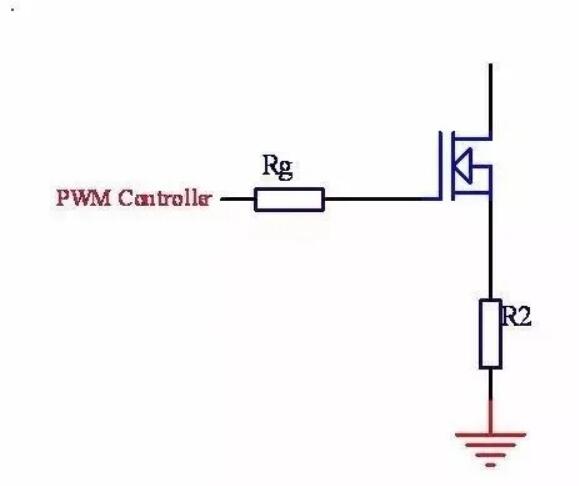
Of course, another problem we have to consider is the driving capability of PWM CONTROLLER. When the MOSFET is large, the driving capability of IC is small, and there will be problems such as too slow driving, too large switching loss or even inability to drive. We need to pay attention to this when designing.
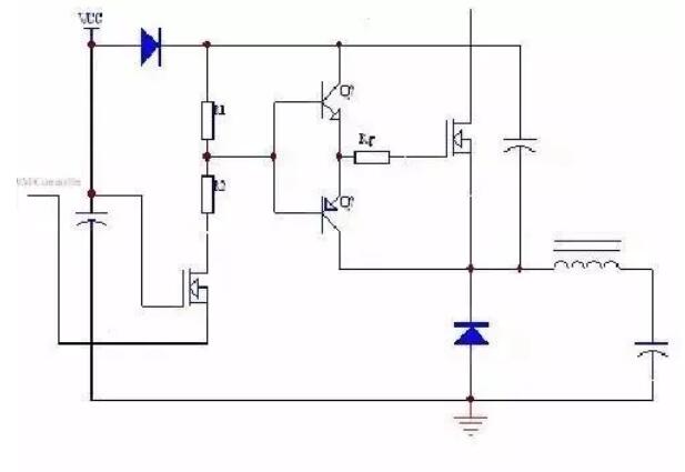
Of course, we can also use the following methods to solve the problem of insufficient internal driving capability of IC.
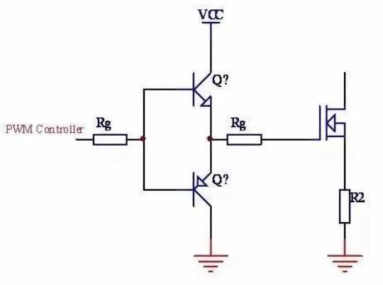
This way of increasing driving capability not only increases the on time, but also accelerates the off time, and at the same time, it has certain effect on controlling burr and power loss. Of course, we should try our best to place these two tubes near the gate of MOSFET in LAYOUT. This has the advantage of reducing parasitic inductance and improving the anti-interference performance of the circuit.
If we only want to increase the turn-off speed of MOSFET, then we can do it in the following way.
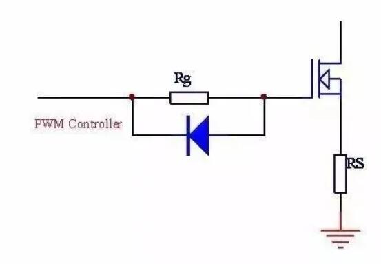
When the turn-off current is large, the discharge speed of MOSFET input capacitor can be faster, thus reducing the turn-off loss. High discharge current can be achieved by selecting MOSFET with low output impedance or negative voltage device with N-channel cut-off, the most commonly used one is adding accelerating diode.
When the gate is turned off, the voltage drop caused by the current on the resistor is greater than that of the diode when it is turned on, and then the diode will turn on, thus bypassing the resistor. After turning on, with the decrease of the current, the role of the diode in the circuit becomes smaller and smaller, which will significantly reduce the delay time of turning off the MOSFET.
Of course, this circuit has a certain disadvantage, that is, the current at the gate still needs to pass through the output drive impedance inside the IC. What can be done to solve this problem?
Let's talk about the PNP accelerated shutdown drive circuit:
Let's talk about the following PNP accelerated shutdown circuit.
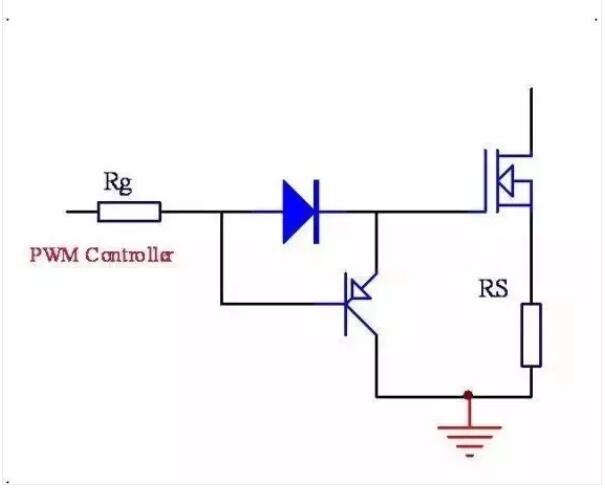
The PNP turn-off circuit is the most widely used circuit at present, which can realize the instantaneous gate-source short circuit under the action of the accelerating diode, thus achieving the shortest discharge time. The reason why the diode is added is to protect the base of the diode on the one hand, and to provide a circuit and bias for the conduction current on the other. The advantage of this circuit is that it can achieve the push-pull effect approximately, and the acceleration effect is obvious. The disadvantage is that the gate can't really reach 0 volts because it passes through two PN sections.
When the source output is high voltage, we need to use the bias circuit to achieve the purpose of circuit operation, that is, we set up the bias circuit with the source as the reference point, the driving voltage fluctuates between two voltages, and the deviation of the driving voltage is provided by the low voltage, as shown in the following figure.
Of course, there is something wrong with this picture. I wonder if any heroes can see it?
Actually, the problem is that the "driving power supply" needs to be suspended, and the source of MOS should be "grounded" (to impress everyone)
This is the correct drawing. For your reference:
In order to meet the requirements of safety isolation or provide high-end floating gate drive, transformer drive is often used. This drive isolates the drive control from the MOSFET and can be applied to low-voltage and high-voltage circuits, as shown in the following figure:
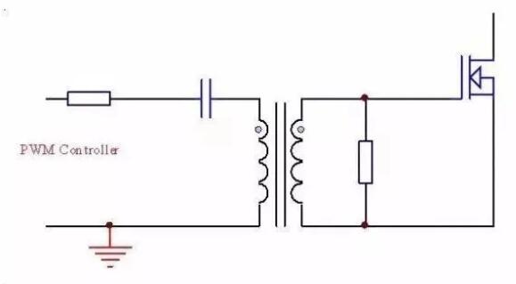
To put it bluntly, transformer drive is isolated drive. Now, of course, there are special driver IC to solve it, but transformer drive has its own characteristics, which makes many people insist on using it all the time.
The function of the coupling capacitor in the figure is to provide reset voltage for the magnetized magnetic core. Without this capacitor, magnetic saturation will occur.
The function of the resistor connected in series with the capacitor is to prevent the sudden change of duty cycle from causing LC oscillation, so this resistor is added to relieve it.
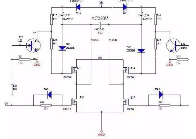
The following actual bootstrap inverter diagram is for reference:
Disclaimer: This article is reproduced from "Electronic Hardware Application Technology". This article only represents the author's personal views, and does not represent the views of Sacco Micro and the industry. It is only for reprinting and sharing to support the protection of intellectual property rights. Please indicate the original source and author when reprinting. If there is any infringement, please contact us to delete it.
Company Tel: +86-0755-83044319
Fax/fax:+86-0755-83975897
Email: 1615456225@qq.com
QQ: 332496225 Manager Qiu
Address: Room 809, Block C, Zhantao Technology Building, No.1079 Minzhi Avenue, Longhua New District, Shenzhen


Site Map | 萨科微 | 金航标 | Slkor | Kinghelm
RU | FR | DE | IT | ES | PT | JA | KO | AR | TR | TH | MS | VI | MG | FA | ZH-TW | HR | BG | SD| GD | SN | SM | PS | LB | KY | KU | HAW | CO | AM | UZ | TG | SU | ST | ML | KK | NY | ZU | YO | TE | TA | SO| PA| NE | MN | MI | LA | LO | KM | KN
| JW | IG | HMN | HA | EO | CEB | BS | BN | UR | HT | KA | EU | AZ | HY | YI |MK | IS | BE | CY | GA | SW | SV | AF | FA | TR | TH | MT | HU | GL | ET | NL | DA | CS | FI | EL | HI | NO | PL | RO | CA | TL | IW | LV | ID | LT | SR | SQ | SL | UK
Copyright ©2015-2025 Shenzhen Slkor Micro Semicon Co., Ltd
