Service hotline
+86 0755-83044319

release time:2022-03-17Author source:SlkorBrowse:11024
Recently, I read the article by Professor Chen Yongzhen of Liaoning University of Technology, "Is electrolytic capacitor for GaN FET just a gimmick?" There are a lot of feelings, so the electrolytic capacitor for gallium nitride (GaN)FET (field effect transistor) came into being. Apart from its reduced volume, its parasitic inductance can't be greatly reduced when the manufacturing process has not changed substantially, and it has inductance characteristics at high switching frequency, with abundant higher harmonics. Therefore, such an electrolytic capacitor is unnecessary.
+Indeed, at the moment of iteration of a new generation of innovative technologies, there will always be mud and sand. However, with the development of new technology's peripheral supporting technology, its role will be more and more important, such as gallium nitride power devices. Let's take a look at what the big coffee makers in the industry have said about gallium nitride recently, and what lessons can they give us?
GaN has become a 5G energy catalyst.
"The emergence of gallium nitride will meet the demand of 5G, realize a new topology, and completely change fast charging," said Stephen Oliver, vice president of corporate marketing and investor relations at Navitas Semiconductor.
According to the data released by GSMArena, since 2010, the average screen size and battery capacity of new mobile phone platforms such as Apple iPhone 12, Xiaomi Mi11 and Samsung S21 have increased by more than three times. It is unacceptable to use slow silicon-based 5W or 20W commercial chargers to prolong the charging time, so more power is needed.
As the traditional low-frequency topology shows, getting more energy from the silicon charger means larger size, heavier weight and higher cost, and the design of power density and thermal density are bottlenecks.
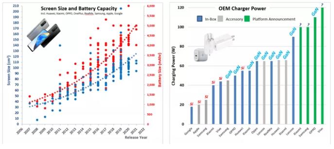
Within 10 years, the screen size and battery capacity of smart phones have increased by more than 3 times.
Oliver said that the increase of smartphone screen, battery and 5G functions, as well as the enhancement of data processing and transmission rate and capacity, made people pay attention to charging speed and the size, weight and cost of travel adapter. At the same time, the introduction of a single, flexible charging platform (hardware and software), namely USB-C connector (USB-C) or programmable power supply (PPS) with power transmission (USB-PD), means that consumers no longer rely on power products provided by OEM.
He believes that the key to improving power density is to increase switching frequency and minimize passive components such as transformers, EMI filters, large capacity and output capacitors. As early as 1996, a high-speed topology such as Active Clamped Flyback (ACF) was proposed by the academic community, but it was frustrated by the poor on-resistance and switching performance and complexity of silicon and the lack of optimal control IC.
At the beginning of 2018, the introduction of GaN power IC put an end to this situation, which not only made ACF commercially feasible, but also made high-frequency quasi-resonant flyback charging of smartphone charger, as well as CrCM (critical conduction mode) boost PFC (power factor correction) topology, high-speed LLC (resonant controller) and advanced CrCM totem pole PFC for higher power systems such as gaming notebook computers, integrated PCs, televisions and 5G transmitting unit power supplies commercially feasible.
GaN power IC integrates GaN power FET and GaN driver plus control and protection in one chip package. These GaNFast™ power supply ICs are easy-to-use, high-speed and high-performance digital input and output power supply components. Because the gate drive circuit basically has no impedance, there is almost no loss when it is turned off after integration. In addition, the opening performance can be controlled and customized according to specific application requirements.
What's the effect? GaN power IC runs 20 times faster and 3 times higher than traditional silicon design, and has been used by OEMs such as Dell, Lenovo and Xiaomi to quickly charge smart phones and laptops. As can be seen from the OPPO 50W Mini SuperVOOC Cookie Quick Charger, the high-speed GaN topology eliminates passive components and reduces the size of the charger. With TI UCC28782 controller and a pair of half-bridge configuration GaNFast power ics, high efficiency active clamp flyback with 10 times faster speed is realized.
Testing under harsh market demand

图源 | 网络
“Careful voltage and temperature stress tests show that GaN power devices have high reliability required by the automotive and industrial markets, "said Ron Barr, vice president of quality and reliability of Transphorm.
The advantages of wide band gap (WBG) GaN power MOSFET make it play an increasingly important role in demanding occasions such as automobile power subsystem and data center power supply. These applications have challenging working conditions, and failures cannot be tolerated due to automobile warranty costs or high costs related to data center reliability. When selecting power devices, design engineers must be sure that they are reliable, strong and durable.
Taking the depletion GaN HEMT (high electron mobility transistor) TP65H035WSQA designed by Transphorm normally-off dual-chip as an example, the GaN HEMT and a normally-off low-voltage silicon FET are connected in series to form a cascode device structure.
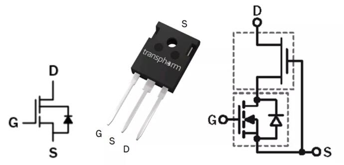
Cascode symbol and cascode device combination structure
The device is packaged in TO-247 and meets AEC-Q101 standard at 175℃. When evaluating product reliability, design engineers need four "domains" of reliability information/data to determine whether the device is suitable for application, including: product certification; Highly accelerated life test; Early life failure test; Field reliability.
产品认证
Product certification mainly follows two common standards in the industry. JEDEC JESD 47 is suitable for commercial devices, and stricter AEC-Q101 standard is suitable for vehicle gauge devices. Each standard has a series of tests that products must pass, such as temperature cycling, high-temperature reverse bias, high-temperature grid bias, etc., so that such products can be regarded as JEDEC or Q101 qualified.
高加速寿命试验
Highly accelerated life test (HALT) is a well-defined method, that is, the stress is applied to the device under the condition that it sometimes exceeds the limit of its data sheet until the device fails. At the same time, the data about the time to failure (TTF) is collected, so that an appropriate model can be applied to predict the durable life (also called the inherent life).
Under reverse bias, a batch of 650V rated voltage devices with voltages between 1050V and 1150V in the off state were tested until most devices failed. Then calculate the average time to failure under each set of conditions.
图源 | The Verge
In a similar way, the device should be tested for failure at three different temperatures. Three different voltages and three different temperatures are obtained under accelerated test conditions. Now, the failure time of each test is normalized under a set of usage conditions, which are usually derived from the application task summary. In the example, a set of extreme conditions are selected to calculate the lifetime of 650V 175℃ device with 100% duty cycle.
All the test data can be combined in a model, which is called "usage graph". This graph shows the failure probability plotted according to the failure time under the usage conditions.
The common practice is to define the device life when the failure probability is 100PPM. In this example, it is 106 hours of continuous operation for 100 years.
早期失效试验
Early failure test is used to calculate the warranty risk in application and test the probability of failure before the device is damaged. Early life failure (early failure rate) usually occurs due to defects not found or screened out in the manufacturing process, which is usually called "internal defects". In the case of GaN devices, these inherent defects will lead to electric field distortion and accelerated failure of defect positions.
In order to test meaningfully, we should try to test a device sample much larger than the HALT test described before, so as to increase the probability of finding intrinsic defects. The method of using is fully described in JEDEC standard JESD 74A, which can be obtained on JEDEC website.
Early life failure is usually calculated by FIT (Billion Hour Failure Rate) or PPM/ year. The data shows that the FIT rate is very low, which may indicate very good field reliability.
现场可靠性
Transphorm's on-site reliability calculation follows the industry practice, and takes into account the number of delivered devices, how long it will be used in the field, and how many devices have failed as reported by customers. Of course, not all products can be delivered or used immediately. To be conservative, the total number of device hours will be halved. The working time of Transphorm's devices in the field is far more than 7 billion hours. So far, it has been returned twice, and its field reliability is less than 1FIT.
“Tests show that the above GaN power devices exceed the challenging reliability requirements of automobile and industrial OEMs. The reliability of these GaN devices is at least equal to that of existing silicon and other wide bandgap technologies, and it is often better, "Barr confidently concluded.
GaN栅极驱动的新要求
图源 | Pinterest
"Low power consumption GaN is the next revolutionary step, which will open up a new era for power electronics applications. However, some problems need to be paid attention to when using the new power transistor technology, "Eric Persson, senior chief engineer of Infineon Technology, pointed out.
The power switch plays an important role in improving the performance, density and cost of the adapter. Traditionally, power transistors used as switches are silicon-based, and the trend clearly shows that wide bandgap transistors, especially GaN, are becoming the standard of high performance and small size adapters.
Looking back at the development of power transistor technology, until today, silicon SJ (super junction) transistor has been the main transistor technology used in charger/adapter. It can provide low on-resistance, excellent current handling capability, simple gate driving, and time-proven reliability in a small package, all of which are low-cost.
However, considering the wide voltage range required by the adapter and overvoltage transient caused by leakage inductance and lightning surge transient, even 650V transistors are often not enough, requiring 700-800V devices. And this is one aspect in which GaN has obvious advantages over silicon. Because, when the applied voltage exceeds the rated voltage, the silicon transistor will enter the avalanche breakdown state. Some designs use Zener effect as buffer to suppress overvoltage transient. However, even if the energy is in the safe working area (SOA) of the transistor, this method will increase the power loss, and may lead to additional undesirable EMI (electromagnetic interference). In addition, a large amount of energy generated by surge may exceed avalanche energy and damage the transistor.
On the contrary, the rated voltage of GaN transistor is much lower than its actual destructive breakdown voltage. The rated voltage of the transistor is based on the specified application conditions to meet the reliability level required for the device life. E-type HEMT of coolgan 600v, for example, usually has a destructive breakdown voltage of more than 1000V, and its pulse voltage rating is 750V under various conditions. In the perfect ACF matching topology, the leakage energy is managed by the resonant circuit, and the high pulse voltage rating of GaN can adjust the lightning surge voltage.
The key to the application of GaN transistor is that its gate drive requirements are different from those of silicon transistor. An important difference is that the threshold and all-on gate-source voltage (VGS) of GaN are significantly lower than those of silicon transistors. Although this reduces the gate charge, it may also present challenges in keeping the transistor off. In ACF circuit, two transistors are configured as half-bridges, the main switch is at the bottom, and the active clamp is used as the high-side switch. And the controller and the low-side transistor driver are powered by a bias power supply. But the high-side gate driver needs a floating power supply. In large telecom or data center power supply, a single DC-DC converter can be used to provide floating bias power for the high voltage side. But in the adapter/charger, the size and cost of this method are prohibitive.
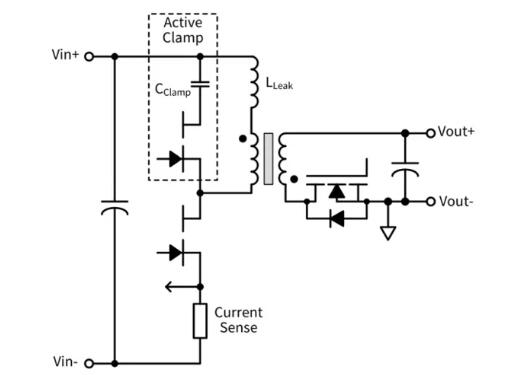
Active clamp flyback topology simplified circuit
A common method of supplying power to the high-voltage side is the so-called bootstrap power supply, that is, when the low-voltage side is turned on, the energy storage capacitor biased by the high-voltage side is charged upward from the low-voltage side bias power supply through a diode. When the high voltage side is opened, it will draw bias from the energy storage capacitor, and it must be replenished regularly (every time the low voltage side is opened). When the circuit works continuously, this is a very effective and low-cost method to supply power to the high-voltage side. But the challenge is how to operate in discontinuous mode.
So, how to avoid the false turn-on of the high side when the bootstrap capacitor is not charged? The general gate driver IC of sometimes includes a clamping circuit design, but the traditional method for silicon transistors relies on a higher threshold voltage (such as 3-4V). Therefore, if the circuits start clamping in the range of 1-2V, unfortunately, they need hundreds of ns to start clamping. GaN transistors can already conduct a large amount of current at these gate voltages.
In order to optimize the performance of fast clamp driver combined with GaN transistor, the interference impedance between them must be minimized. Yingling adopts the method of integrating high-side and low-side GaN transistors (190mΩ), and integrates them with a new half-bridge driver in an iQFN 8×8mm package, thus making a half-bridge integrated power stage (IPS).
Compared with competitive products, this integration and partition method has the following advantages:
No external digital isolator is needed, and the propagation delay is very short (47ns)
The mismatch time of the delay between the high and low side drivers is only a few ns, so the dead zone time can be safely and easily adjusted to the minimum to obtain the best efficiency.
The RC (resistance-capacitance) network of the gate is driven externally, which allows the switching speed to be adjusted to balance the loss and EMI. The capacitance through the isolation gate is very small, which reduces the common-mode EMI current.
High-side and low-side drivers are completely isolated
写在最后
发挥优势的时刻已经到来
The third-generation semiconductors represented by gallium nitride and silicon carbide have excellent characteristics such as high temperature resistance, high voltage resistance, high frequency, high power and radiation resistance, and the limitations in technology and cost are slowly melting away. Next, it depends on how the application side can give full play to its advantages through device testing, driver development and peripheral component matching.
Disclaimer: This article is reproduced from "and non-web eefocus". This article only represents the author's personal views, and does not represent the views of Sacco Micro and the industry. It is only for reprinting and sharing to support the protection of intellectual property rights. Please indicate the original source and author when reprinting. If there is any infringement, please contact us to delete it.


Site Map | 萨科微 | 金航标 | Slkor | Kinghelm
RU | FR | DE | IT | ES | PT | JA | KO | AR | TR | TH | MS | VI | MG | FA | ZH-TW | HR | BG | SD| GD | SN | SM | PS | LB | KY | KU | HAW | CO | AM | UZ | TG | SU | ST | ML | KK | NY | ZU | YO | TE | TA | SO| PA| NE | MN | MI | LA | LO | KM | KN
| JW | IG | HMN | HA | EO | CEB | BS | BN | UR | HT | KA | EU | AZ | HY | YI |MK | IS | BE | CY | GA | SW | SV | AF | FA | TR | TH | MT | HU | GL | ET | NL | DA | CS | FI | EL | HI | NO | PL | RO | CA | TL | IW | LV | ID | LT | SR | SQ | SL | UK
Copyright ©2015-2025 Shenzhen Slkor Micro Semicon Co., Ltd
