Service hotline
+86 0755-83044319

release time:2022-03-17Author source:SlkorBrowse:12371
Connected with the strongest chip industry chain science popularization, the depth analysis of chip self-controllable (1)
Etching machine
Etching is the process of removing unnecessary materials from the wafer surface. Etching is performed after photolithography.Mask aligner light is used to copy the circuit structure on the mask onto the silicon wafer, and the etching machine micro-carves the circuit structure copied onto the silicon wafer, carving grooves and contact points so that the circuit can be put in.According to the etching process, it can be divided into dry etching and wet etching. The dry etching mainly uses reactive gas and plasma for etching, while the wet etching process mainly involves soaking etching materials in etching solution for etching.Dry etching is the mainstream in semiconductor etching, accounting for 95% of the market. Its biggest advantage is that it can realize anisotropic etching, that is, it can control only the materials in the vertical direction to be etched without affecting the materials in the horizontal direction, thus ensuring the fidelity of fine graphics. Due to uncontrollable etching direction, wet etching can easily reduce the line width and even destroy the circuit itself in advanced processes, resulting in poor chip quality.At present, the principle of multi-template process is widely adopted, that is, the required feature size is achieved by multiple deposition and etching processes. For example, the etching steps required for 14nm process reach 64 times, which is 60% higher than that for 28nm. The etching steps required for 7nm process are as high as 140 times, which is 118% higher than that for 14nm.The following figure shows the principle of multiple etching.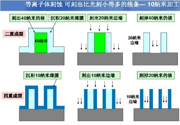
Like mask aligner, there are relatively few etching machine manufacturers, and the representative enterprises are Lam Research (Pan Lin Semiconductor), AMAT (Applied Materials) and TEL (Tokyo Electronics) in the United States. These three companies account for 94% of the global market share of semiconductor etchers, while other participants only account for 6%. Among them, Lam Research accounts for as much as 55%, which is the industry leader, and Tokyo Electronics and Applied Materials account for 20% and 19% respectively.At present, the representative companies of etching equipment are Zhongwei Company, North Huachuang Company, etc. China Micro Company is a leader, and the process node has reached 5nm. Among the top ten wafer companies in the world, China Micro Company has entered six of them, and as a partner of [敏感词], it has cooperated to verify advanced technologies such as 14nm/7nm/5nm.
2.2 Process
The manufacturing process of the chip requires more than 2,000 technological processes. Below, we briefly introduce the chip manufacturing process according to the eight steps.
1.Lithography (optical development)
Lithography is the process of exposure and development, which converts the pattern on the mask to the wafer under the photoresist. Lithography mainly includes photoresist coating, baking, mask alignment, exposure and development. Exposure methods include: ultraviolet, extreme ultraviolet, X-ray, electron beam, etc.
2.Etching (etching)
Etching is a technique of removing materials by chemical reaction or physical impact. Dry etching uses the physical action produced by plasma striking the wafer surface, or the chemical reaction between plasma and atoms on the wafer surface, or the combination of both. Wet etching uses chemical solution, and achieves the purpose of etching through chemical reaction.
3. Chemical vapor deposition (CVD)
Chemical reactions such as CVD heat energy, discharge or ultraviolet light irradiation are used to deposit reactants on the wafer surface to form a stable solid film. CVD technology is widely used in chip manufacturing, such as dielectrics materials, conductors or semiconductors, etc., which can be completed by CVD technology.
4. Physical vapor deposition (PVD)
PVD is a physical process rather than a chemical process. Generally, argon and other gases are used. After argon ions are accelerated in vacuum to hit the sputtering target, the target atoms can be sputtered out one by one, and the sputtered materials can be deposited on the wafer surface like snowflakes.
5. Ion Implant (ion implant)
Ion implantation can implant dopants into specific areas of semiconductor components in ion form to obtain accurate electrical characteristics. The ions are accelerated to sufficient energy and speed to penetrate (implant) the thin film and reach a predetermined implantation depth. Ion implantation can precisely control the dopant concentration in the implanted region.
6. Chemical mechanical polishing (CMP)
Chemical polishing technology has two functions: mechanical polishing of abrasive substances and chemical polishing of acid-base solutions, which can make the wafer surface completely planarized, so as to facilitate the subsequent film deposition.
7. wash
The purpose of cleaning is to remove metal impurities, organic pollution, dust and natural oxides; Reduce the surface roughness; Almost all processes need to be cleaned before and after.
8. Die Saw
Wafer cutting is to cut and separate the die on the processed wafer, which is convenient for the subsequent packaging test.
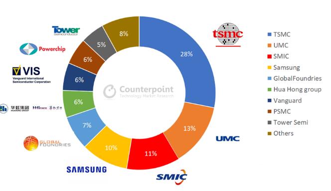
It can be seen that the top four manufacturers in mature process capacity are [敏感词] (market share 28%), UMC (13%), SMIC (11%) and Samsung (10%). The mature process will be very popular in 2020, and the production capacity will be seriously short, which will bring huge business opportunities to major wafer foundries. Judging from the industrial development situation in 2021, this shortage will not be alleviated in the near future.
2.3 material
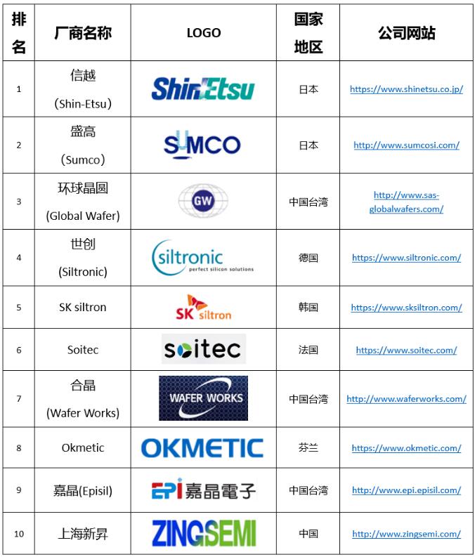 Domestic situation, the average annual compound growth rate of semiconductor silicon wafer sales in Chinese mainland reached 41.17%, far higher than the global semiconductor silicon wafer market of 25.75% in the same period. However, this market is not in the hands of local manufacturers, and there is still a lot of room for domestic wafer manufacturers to develop in today's domestic industrial chain.
Photoresist is the most important consumable in lithography process, and the quality of photoresist has an important influence on lithography process. Photoresist can be divided into semiconductor photoresist, panel photoresist and PCB photoresist. Among them, semiconductor photoresist has the highest technical barrier. At present, the main photoresist companies in the world are Japan Synthetic Rubber (JSR), TOKyo Yinghua (Tok), ShinEtsu Chemical (Shinetsu), FUJI Electronics (Fuji), Rohm&Hass of the United States, etc., and their market concentration is very high, accounting for more than 85% of the market. The following figure shows the market share of photoresist enterprises. High-resolution semiconductor photoresist is the material with the highest technical barrier among semiconductor chemicals, and the technology of Japanese and American enterprises is twenty to thirty years ahead of that of domestic enterprises. From the perspective of photoresist technology level, domestic enterprises have explored a road of independent research and development under the conditions of lack of experience, professional and technical talents and key upstream raw materials and equipment. It is still difficult to break through the high-end photoresist technology in a short time, and there is still a long way to go. In the field of PCB, domestic photoresist has a certain mass production capacity and has been supplied to mainstream manufacturers.
03
Packaging test
3.1 chip packaging
We analyze chip packaging from two aspects: packaging design and product packaging.
There is no concept of Integration in the previous packaging, and the packaging design is relatively simple, with low requirements for tools. Auto CAD is a commonly used packaging design tool. With the emergence of MCM and SiP technologies, the packaging design has become more and more complex. In addition, the market acceptance of SiP, advanced packaging, Chiplet and heterogeneous integration concepts is getting higher and higher, and the complexity and flexibility of the integration within the package have risen sharply, and the requirements for the packaging design have become higher and higher.At present, there are only Cadence and Siemens EDA(Mentor) for SiP and advanced packaging design tools. Cadence is an established EDA provider of packaging design, which has a high market share and high loyalty of users.Siemens EDA(Mentor) is a rising star in the field of packaging design, but its technological advancement reflects the characteristics of "the late wave". Industry leaders [敏感词], Intel, SAMSUNG have chosen Siemens EDA as their first choice tool for advanced packaging (HDAP), which mainly lies in two aspects: advanced design tools and powerful verification tools.First of all, let's talk about design tools. In a technical forum, I said, "Different from traditional packaging design, advanced packaging and SiP design have high requirements for 3D environment. The 3D design environment lies not in whether it looks intuitive and gorgeous, but in the accurate description of objective elements, including bonding wires, cavities, chip stacks, silicon adapter boards, 2.5D integration, 3D integration, Bump ..."At this point, Siemens EDA's SiP and advanced package design tools have left its competitors far behind. The following figure is a 3D screenshot of the package design in XPD, an advanced package layout design tool. In four groups of chip stacks, each group of five chips (4HBM+1Logic) are connected together by 3D TSV, and integrated with GPU on a silicon adapter board (2.5D TSV), which is integrated with resistors, capacitors, etc. on the package substrate.
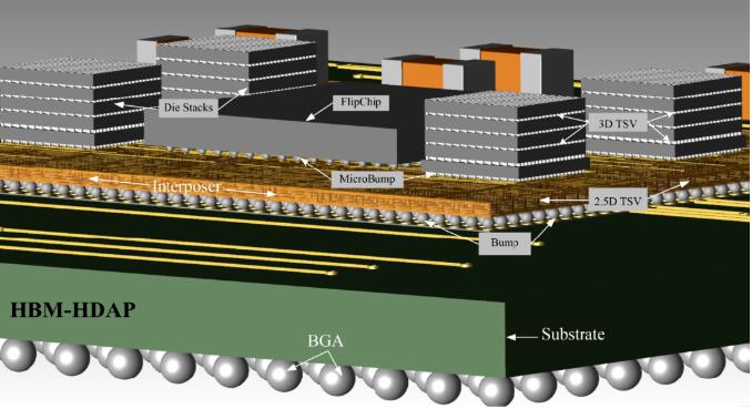
Screenshot of advanced package design in XPD (3D)This design includes 3D integration, 2.5D integration, flip-chip, Bump, multi-substrate integration, etc., which has been accurately realized in XPD design environment. Advanced package verification tools include electrical verification and physical verification. Electrical verification contains more than 80 rules, which check and verify the whole system in terms of signal integrity, power integrity, EMI\EMC and other electrical aspects. Physical verification is based on IC verification tool Calibre, which integrates Calibre 3D STACK and is specially used for physical verification of 3D advanced packages. With the increasing integration and design complexity in the package, the requirements for tools are higher and higher. In addition, in the field of advanced packaging, the synergy between package design and chip design is increasing, and there is a trend of gradual integration to some extent, so the requirements for collaborative design are also increasing. For detailed design methods and practical cases of SiP, microsystem and advanced packaging, please refer to the new book "Microsystem Based on SiP Technology" to be published by Electronic Industry Press.2) According to different materials and processes, product packaging can be divided into three types: plastic packaging, ceramic packaging and metal packaging. Plastic packaging is mainly based on organic substrates, and is mostly used in commercial products. It is small in size, light in weight and cheap, and has the advantages of mass production and low cost, but it is relatively poor in heat dissipation, stability and air tightness of chips. Ceramic packaging and metal packaging are mainly based on ceramic substrates. HTCC substrates are generally used for ceramic packaging, while LTCC substrates are mostly used for metal packaging. For high power consumption products, aluminum nitride substrates can be used. Ceramic packaging features include: good sealing performance, good heat dissipation performance, good resistance to extreme temperature, easy disassembly and easy problem analysis; Compared with metal packaging, it is relatively small in size, suitable for large-scale complex chips, and suitable for severe environmental applications such as aerospace and the like that require air tightness; But the price is expensive, the production cycle is long, and the weight and volume are larger than those of similar plastic products. Metal packaging features include: good sealing, good heat dissipation, easy disassembly and high flexibility; However, due to its relatively large volume, small number of pins, unsuitable for complex chips, high price, long production cycle, complex process and the need to assemble metal shell and substrate, it is mostly used in MCM design and widely used in aerospace field. Both ceramic and metal packages have cavity structures, which are detachable, easy to find faults and "zero" problems, so they are welcomed by users in aerospace and other fields.

3.2 chip testing
Test machine
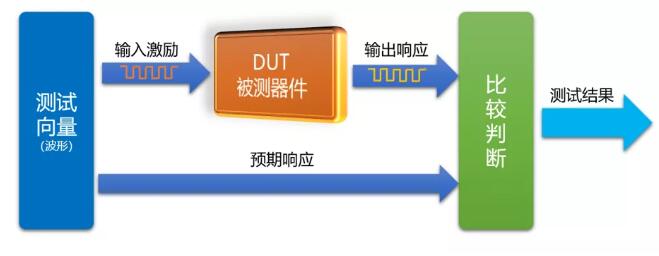
system test
Self-controllable summary
Finally, combined with the following table, we make a simple summary of autonomy and controllability.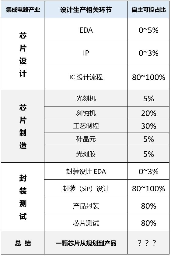
Only by truly recognizing one's own shortcomings, seeking truth from facts, being steadfast, one step at a time, and persevering, can we not fall behind in the fierce competition, thus reducing the occurrence of neck sticking!
Disclaimer: This article is reproduced from "The Analects of Confucius". This article only represents the author's personal views, and does not represent the views of Sacco Micro and the industry. It is only for reprinting and sharing to support the protection of intellectual property rights. Please indicate the original source and author when reprinting. If there is any infringement, please contact us to delete it.
Company Tel: +86-0755-83044319
Fax/fax:+86-0755-83975897
Email: 1615456225@qq.com
QQ: 3518641314 Manager Li
QQ: 332496225 Manager Qiu
Address: Room 809, Block C, Zhantao Technology Building, No.1079 Minzhi Avenue, Longhua New District, Shenzhen


Site Map | 萨科微 | 金航标 | Slkor | Kinghelm
RU | FR | DE | IT | ES | PT | JA | KO | AR | TR | TH | MS | VI | MG | FA | ZH-TW | HR | BG | SD| GD | SN | SM | PS | LB | KY | KU | HAW | CO | AM | UZ | TG | SU | ST | ML | KK | NY | ZU | YO | TE | TA | SO| PA| NE | MN | MI | LA | LO | KM | KN
| JW | IG | HMN | HA | EO | CEB | BS | BN | UR | HT | KA | EU | AZ | HY | YI |MK | IS | BE | CY | GA | SW | SV | AF | FA | TR | TH | MT | HU | GL | ET | NL | DA | CS | FI | EL | HI | NO | PL | RO | CA | TL | IW | LV | ID | LT | SR | SQ | SL | UK
Copyright ©2015-2025 Shenzhen Slkor Micro Semicon Co., Ltd
