Service hotline
+86 0755-83044319

release time:2022-03-17Author source:SlkorBrowse:12128
In 1947, American physicists shockley, Badin and bratton jointly invented the transistor, a semiconductor solid element with three pivots.
Because transistors have the characteristics of low power consumption, small size, relatively cheap price and flexible connection mode, after the advent of transistors, many functions that could not be realized before have been realized in electronic circuits, especially pulse circuits and digital circuits. Let's take a look. The following video is intuitive and thorough, and it is an excellent work for learning popular science. I suggest you have a look (with translation)!(Video source: TEDEd, translation: @ turboxiaozhou)
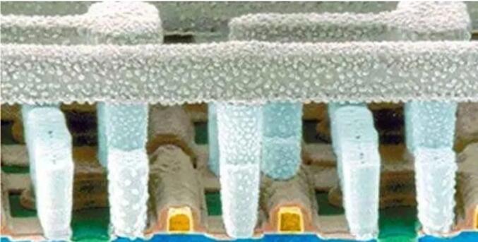
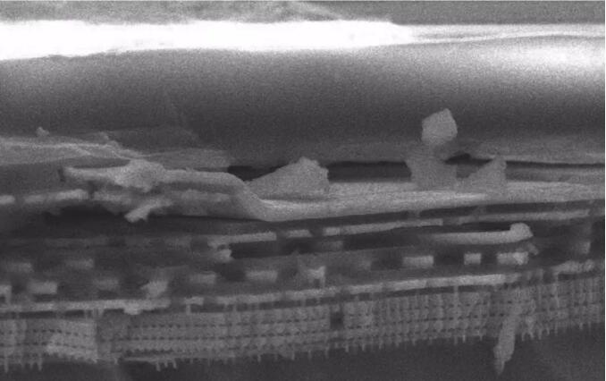
Chip cross section

This is the cross-sectional view of the CPU. You can clearly see the layered CPU structure. The chip is arranged in a hierarchical way. This CPU has about 10 layers. The lowest layer is the device layer, which is the MOSFET transistor.
When the Mos tube is enlarged in the chip, a three-dimensional structure like a "platform" can be seen, and the transistor has no inductance, resistance and other devices which are easy to generate heat. The top layer is a low-resistance electrode, which is separated from the lower platform by an insulator. Generally, P-type or N-type polysilicon is used as the raw material of the gate, and the lower insulator is silicon dioxide.
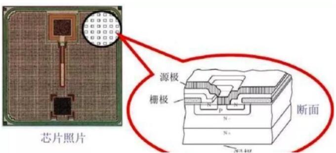
The two sides of the platform are the source and drain by adding impurities, and their positions can be interchanged. The distance between them is the channel, which determines the characteristics of the chip.
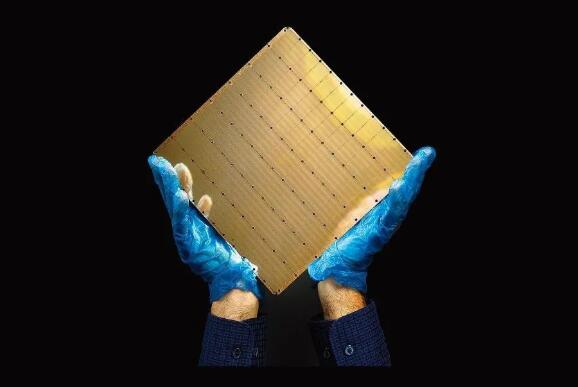
Chip with 2.6 trillion transistors, from Cerebras Systems
Of course, the transistors in the chip are not only Mos transistors, but also tri-gate transistors. The transistors are not installed, but carved when the chip is manufactured.
Disclaimer: This article is reproduced from "Semiconductor Online". This article only represents the author's personal views, and does not represent the views of Sacco Micro and the industry. It is only for reprinting and sharing to support the protection of intellectual property rights. Please indicate the original source and author when reprinting. If there is any infringement, please contact us to delete it.
Company Tel: +86-0755-83044319
Fax/fax:+86-0755-83975897
Email: 1615456225@qq.com
QQ: 3518641314 Manager Li
QQ: 332496225 Manager Qiu
Address: Room 809, Block C, Zhantao Technology Building, No.1079 Minzhi Avenue, Longhua New District, Shenzhen


Site Map | 萨科微 | 金航标 | Slkor | Kinghelm
RU | FR | DE | IT | ES | PT | JA | KO | AR | TR | TH | MS | VI | MG | FA | ZH-TW | HR | BG | SD| GD | SN | SM | PS | LB | KY | KU | HAW | CO | AM | UZ | TG | SU | ST | ML | KK | NY | ZU | YO | TE | TA | SO| PA| NE | MN | MI | LA | LO | KM | KN
| JW | IG | HMN | HA | EO | CEB | BS | BN | UR | HT | KA | EU | AZ | HY | YI |MK | IS | BE | CY | GA | SW | SV | AF | FA | TR | TH | MT | HU | GL | ET | NL | DA | CS | FI | EL | HI | NO | PL | RO | CA | TL | IW | LV | ID | LT | SR | SQ | SL | UK
Copyright ©2015-2025 Shenzhen Slkor Micro Semicon Co., Ltd
