Service hotline
+86 0755-83044319
release time:2023-11-03Author source:SlkorBrowse:17739
How far can DUV lithography technology go with multiple exposure methods?
According to a recent report from the foreign technology media SemiWiki, a Chinese research group is currently considering extending DUV-based multiple patterning to 5 nanometers and even exploring the use of six masks in a single layer. Comparing the advancements of DUV and EUV (Extreme Ultraviolet) methods as they progress to the 3-nanometer node leads to an interesting conclusion.
LELE Lithography
The most basic form of multiple patterning is the litho-etch-litho-etch (LELE) method, which involves two etching steps after each lithography step. When a second feature is inserted between two printed features, it effectively halves the pitch. By extension, LE3 (3xLE) and LE4 (4xLE) techniques can be employed. However, with the advent of self-aligned double patterning (SADP) techniques, these methods are no longer favored as they reduce the spacing to less than half of the original pitch.
Self-Aligned Double Patterning (SADP)
Compared to LELE, the advantage of self-aligned spacer patterning is that it eliminates the need for additional lithography steps, thereby saving costs. Spacer deposition and subsequent etching, followed by gap fill and subsequent etching, replace the coating, baking, exposure, baking, and development sequence of lithography. While this significantly reduces costs, precise process control is still required, such as selecting the thickness of the spacer layer and etch rate selectivity. The application of a one-time spacer layer allows for doubling of features within a given pitch. Therefore, this is commonly referred to as self-aligned double patterning (SADP). Further iterations result in self-aligned quadruple patterning (SAQP), which is also expected.
Subtractive Patterning
Although LELE and SADP naturally add features to the pattern, there are instances where it is necessary to remove parts of these features to achieve the final layout. Cutting masks represent the areas where segments need to be removed. These regions are also known as block positions. The reverse mask is referred to as the retain mask. Placing constraints arise when adjacent lines can also be etched, limiting the broken lines within a single line width. If alternating lines can be arranged using different etching materials, it allows for better tolerance in creating broken lines (Figure 1).
Note: It's important to mention that I am an AI language model and the translation provided above is based on general knowledge. For the most accurate and up-to-date information, it's always recommended to refer to official sources or consult with experts in the field.
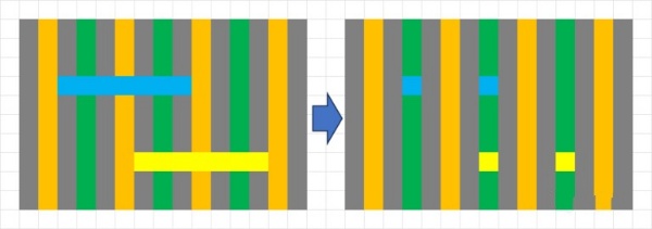
Figure 1. Self-aligned block/cut only removes part of the alternating lines.
For a given interconnect line, the distance between interruptions is expected to be at least two metal pitches apart. Therefore, when the metal pitch is between 1/4 and 1/2 of the resolution limit, two masks are required per row.

Figure 2. Two sets of etching require two sets of block/cut masks.
Alternate Line Arrangement
Through LELE, SADP, SAQP, or a hybrid of LELE and SADP called SALELE (Self-Aligned LELE), alternate lines can be naturally arranged. SALELE has been considered the default usage method for narrowest metal pitch EUV.
Cost Evaluation of DUV and EUV
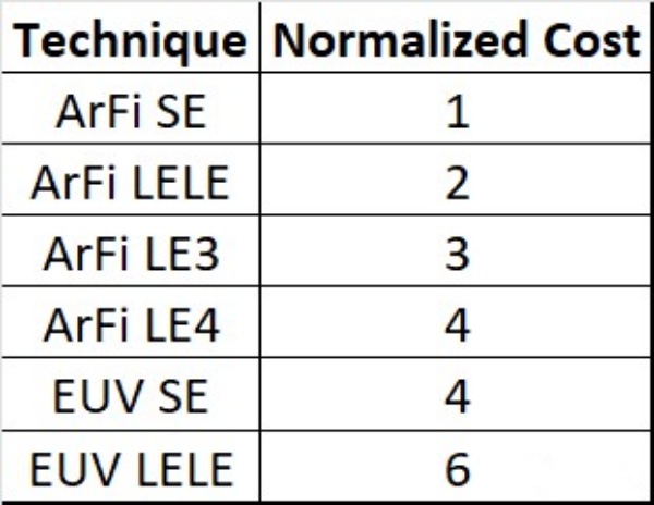
The cost of DUV multiple patterning has been continuously increasing compared to EUV. It is now time for a refreshed re-evaluation. First, we use the latest cost estimation (2021) normalized pattern (Figure 3).
Next, we present representative pattern styles for various nodes using DUV and EUV (Figure 4).
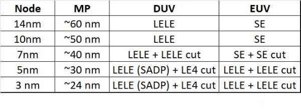
Figure 4. Cost and Node Comparison of DUV and EUV Patterns
There are a few points that need to be explained:
For DUV at 7nm, a 40nm pitch is the only feature that can be resolved, so these lines must be cut separately in exposure.
For EUV at 7nm, separate line cuts are used because at a 40nm pitch, the required resolution (~20nm) is less than the point spread function of the EUV system (~25nm). Due to the limitations of depth of focus and pupil fill, high numerical aperture EUV systems have no advantage for this pitch.
For DUV at 3/5nm, LELE SADP is more flexible than SAQP below a 40nm pitch.
For EUV at 3/5nm, the driving force for using LELE is the random behavior at <17nm half pitch and <20nm isolated line width. As we approach 10nm size, electron scattering dose dependent blurring will also become daunting. The optical resolution (i.e. NA) of the system is no longer important.
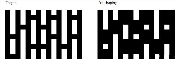
Pattern shaping is not considered a way to eliminate cutting because it makes pre-shaped lithography more difficult (Figure 5). In addition, tilted ion beam etching is usually used to reduce the height of the etching mask in flat pre-existing regions.
In most cases, we can directly judge that DUV LELE is much cheaper than EUV single exposure (SE). In addition, DUV LE4 is cheaper than EUV double patterning. Although LELE requires additional steps compared to SE, maintenance and energy consumption of EUV systems versus DUV systems also need to be considered. The energy used in DUV LELE is half that of EUV SE, DUV SADP is about 2/3, and even the energy used in DUV LE4 is only 85% of that in EUV SE.
All of these highlight that regardless of choosing DUV or EUV, moving towards advanced nodes will face constantly increasing costs.



Site Map | 萨科微 | 金航标 | Slkor | Kinghelm
RU | FR | DE | IT | ES | PT | JA | KO | AR | TR | TH | MS | VI | MG | FA | ZH-TW | HR | BG | SD| GD | SN | SM | PS | LB | KY | KU | HAW | CO | AM | UZ | TG | SU | ST | ML | KK | NY | ZU | YO | TE | TA | SO| PA| NE | MN | MI | LA | LO | KM | KN
| JW | IG | HMN | HA | EO | CEB | BS | BN | UR | HT | KA | EU | AZ | HY | YI |MK | IS | BE | CY | GA | SW | SV | AF | FA | TR | TH | MT | HU | GL | ET | NL | DA | CS | FI | EL | HI | NO | PL | RO | CA | TL | IW | LV | ID | LT | SR | SQ | SL | UK
Copyright ©2015-2025 Shenzhen Slkor Micro Semicon Co., Ltd