Service hotline
+86 0755-83044319
release time:2023-12-19Author source:SlkorBrowse:15121
This article focuses on the design considerations of the drive circuit for silicon carbide (SiC) MOSFETs. It covers topics such as isolation requirements for SiC MOSFET drive, calculation of drive current and drive losses for SiC MOSFETs, basic principles of PCB layout for SiC MOSFET drive current, considerations for parallel design of SiC MOSFETs, parasitic turn-on effects and improvement measures for SiC MOSFETs, considerations for short-circuit protection in SiC MOSFETs, and considerations for packaging of SiC power devices.
I. Isolation Requirements for SiC MOSFET Drive
Silicon carbide MOSFETs are commonly used in high-voltage and high-power applications where isolation between the primary and secondary sides of the power supply is required. In these systems, energy is transferred from one side to the other through a transformer, and the controller is usually placed on one side, such as the secondary side. When driving the SiC MOSFET on the primary side, it is necessary to use isolation to transfer the drive signal from the secondary side controller to the primary side.
By using isolation, the ground of the high-voltage circuit on the primary side and the ground of the controller on the secondary side can be designed independently, avoiding damage to the low-voltage control circuit by the high-voltage circuit. Additionally, unwanted AC or DC signals will not be transmitted from the high-voltage side to the low-voltage side, improving the reliability of the drive circuit. This is a typical requirement for SiC drive circuits.
The traditional method of isolation is optocouplers, which have good transient and noise suppression capabilities but can experience gain variation over time. Another common isolation method is magnetic isolation, but it has limitations in magnetic field environments. Capacitive isolation is also commonly used and has significant advantages in terms of sensitivity to high voltage and external magnetic fields. It also supports fast switching operations with minimal delay. We can discuss the different isolation methods in more detail in subsequent discussions.
II. Calculation of Drive Current and Drive Losses for SiC MOSFETs
In high-voltage and high-power applications, higher drive capability is required to reduce switching losses. Therefore, the drive capability of the driver needs to be evaluated in advance. Generally, for a given switching frequency (freq) and gate charge (Qg) of the SiC MOSFET, the required drive current is freq × Qg. This principle can be used for preliminary selection of the drive chip's drive capability.
Furthermore, assuming N SiC MOSFETs are connected in parallel, each with a gate charge of Qg and a gate drive voltage of VGS, the total drive power is freq × N × VGS × Qg. Based on this, drive losses can be estimated.
In high-voltage and high-power applications, the drain-source voltage DV/DT of SiC MOSFETs can be large, reaching up to 150V/ns. Therefore, for the driver, it is desirable to drive at higher frequencies to minimize the on-state resistance. Additionally, when operating at high voltages, it is important to choose products with larger common mode transient immunity (CMTI). In special cases, certain optimization of the driver's output resistance may be required, which we will discuss later.
III. Basic Principles of PCB Layout for SiC MOSFET Drive Current
When designing the SiC MOSFET drive circuit, similar layout principles to those of ordinary power devices should be followed. Let's briefly review them. From the perspective of parasitic inductance, it is generally recommended to place the SiC MOSFET device and its driver circuit as close as possible to reduce parasitic inductance in the gate drive loop. Additionally, minimizing the parasitic inductance of the power circuit traces can help avoid voltage spikes and noise during MOSFET turn-off.
From the perspective of parasitic capacitance, larger parasitic capacitance between the switch node and ground or a fixed level on the layout will increase switching losses. Therefore, it is advisable to minimize the inter-layer coupling capacitance in PCB layout. Also, try to minimize the overlap between switch nodes and signal lines or voltage buses to avoid the influence of capacitive coupling between PCB layers on signal lines.
From the perspective of electromagnetic interference, power current loops generate high-frequency magnetic field interference, and magnetic components also produce high-frequency magnetic field interference. It is generally recommended to avoid overlap or close proximity between the magnetic field and sensitive signal lines to ensure that the signal lines are not affected. This issue should be considered when dealing with driver circuits, such as the interaction between power switch loops and drive signal lines.
IV. Considerations for Parallel Design of SiC MOSFETs
In high-power applications, parallel connection of MOSFETs is commonly used to increase power capacity. This has been a well-established practice in the era of silicon MOSFETs, whether it is low-voltage MOSFETs in module power supplies or high-voltage MOSFETs of 650V and above in high-voltage and high-power supplies. For SiC MOSFETs, there are some specific design considerations that need to be addressed, which we will discuss in detail.
The main concern when parallelizing SiC MOSFETs is achieving good current sharing. Only with good current sharing can the losses and heat be balanced, preventing them from exceeding the peak current or thermal protection limits. This balancing includes both steady-state and transient conditions. Factors involved include individual device Rdson (on-resistance) and VGS-th (threshold voltage for turn-on) variations, imbalances in device drive voltages, and asymmetry in PCB layout.
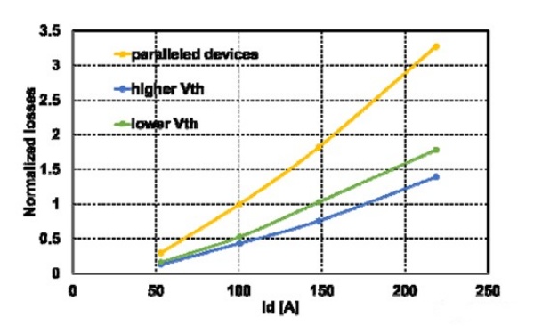
One factor causing imbalance is the different current sharing due to variations in the on-resistance (Rdson) of parallel SiC MOSFETs. This directly leads to different currents flowing through each device, with the MOSFETs with lower Rdson carrying more current and having different conduction losses. If Rdson varies by 20%, the MOSFET with lower conduction impedance would carry 1.5 times the current of the MOSFET with higher conduction impedance, resulting in significant current differences. In addition to conduction loss differences, due to steady-state current differences, there will also be differences in the turn-off losses during switching. The normalized data for turn-off losses of two parallel 1200V 50A SiC MOSFETs are shown in Figure 1 as an example. The Vds specifications and VGS-th specifications of the two devices are basically the same, but Rdson differs by 20%.
Similar to the positive temperature coefficient of on-resistance of silicon MOSFET, the same is true for silicon carbide MOSFET. Therefore, the higher the temperature, the greater the on-resistance and the smaller the current it carries. This characteristic hinders imbalance. Devices that originally bear more current due to the unbalanced Rdson will increase the impedance due to the increase in temperature, thereby reducing the current they bear, so this is a good aspect.
The second factor causing current imbalance is the conduction threshold voltage VGS-th of the silicon carbide MOSFET. If the conduction thresholds of two devices connected in parallel are different, for the same drive signal, the device with the smaller conduction threshold will be turned on first. , and when turned off, this device turns off later, which causes loss or energy imbalance on different devices connected in parallel.
In fact, the VGS-th parameter has a negative temperature coefficient as it changes with temperature. That is to say, the higher the temperature, the lower the conduction threshold. Therefore, one of the devices is too hot due to a different VGS-th. Over time, During operation, the corresponding VGS-th of this hot device will be lower, so the switching time will be longer and it will become hotter, which is a negative aspect for imbalance. Therefore, if the VGS-th difference is large at light load or in applications dominated by switching losses, thermal runaway is particularly likely to occur.

From Figure 2 above, you can see that two 1200V, 50A high-voltage silicon carbide connected in parallel will produce a large turn-off loss due to a certain VGS-th difference (700mV). The conduction loss difference caused by the difference in VGS-th has a small impact. Because of the positive temperature coefficient factor of Rds-on itself, this part of the loss difference can be compensated to a certain extent.
The third aspect that causes unbalance is mainly the driving circuit factors. Generally, in order to reduce switching losses, it is hoped to switch devices at the fastest speed, but the gate-level oscillation problem must also be considered. The gate-level driving resistance Rg and The way the lines are driven is very important to these problems.

Gate-level drive circuits generally have the above recommended methods, [sensitive words] a method of sharing gate-level resistors, without considering other uneven current balancing factors (such as Rds-on, VGS-th, etc.), the drive signal Arrive at the same time, so current sharing is easy, but the RLC resonance generated by the shared drive resistor is prone to gate-level oscillation. In the second method, due to the use of separate gate-level drive resistors, gate-level oscillation is less likely to occur, but due to resistance differences, current imbalance is likely to occur. Therefore, the more recommended method is to use the third method, which has both shared gate-level resistors and separate drive resistors. Combining the [sensitive word] and second methods can achieve better results.
The fourth factor that affects parallel balance is mainly the imbalance of source and drain parasitic inductance caused by layout. As shown in Figure 4, Ld and Ls are the parasitic inductances of the device drain and source respectively.
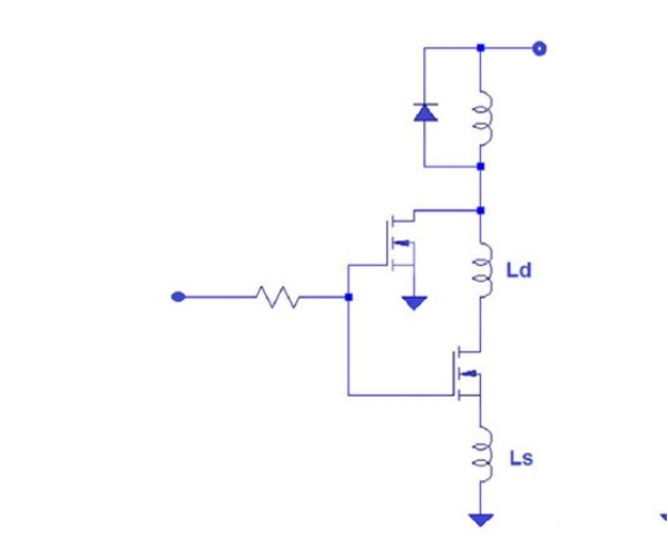
Among them, the Ls parasitic inductance, that is, the unbalanced source parasitic inductance, is the main factor causing the unbalanced current of parallel devices, while the drain inductance has a relatively large impact on the drain voltage stress, which is not within the scope of our discussion this time. Therefore, it is generally recommended to design the source traces as symmetrically as possible to make the source parasitic inductance symmetrical, or reduce its mismatch to avoid current imbalance.
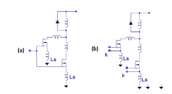
When the device switches, the voltage generated by the larger di/dt on the source parasitic inductance Ls will be fed back to the gate drive circuit. Therefore, when a separate source connection is not used as shown in Figure 5, b, there will be The imbalance of the source voltage will produce additional switching losses and will also lead to a certain gate-level oscillation voltage. When a separate source connection is adopted as shown in Figure 5, b, the influence of the Ls feedback voltage does not need to be considered, and the driving signal will not be added to the source parasitic inductance.
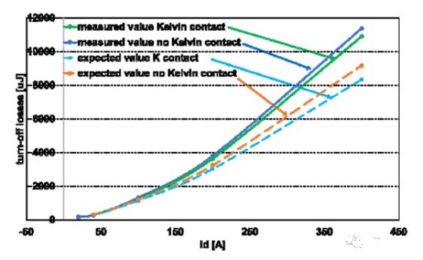
From the graph shown in Figure 6, we can see that when switching losses dominate, the sum of the turn-off losses of a single non-parallel device is smaller than the total turn-off loss of the two devices in parallel. In this sense, the switching loss When it dominates, parallel connection has little significance in reducing losses, but it can effectively average heat distribution. After the above analysis, we can know that when switching losses dominate, since there is no balancing effect of the positive temperature coefficient of Rds-on, if a current imbalance occurs, thermal runaway will easily occur.

If conditions permit, if there is no separate source driver connection, a 1ohm series resistor can be added to the source of the parallel device to achieve dynamic current sharing, which can reduce the di/dt of large drain currents and gate-level The series resistor RGoff can improve the parasitic oscillation caused by the unbalanced parasitic inductance of the source.
To be continued...



Site Map | 萨科微 | 金航标 | Slkor | Kinghelm
RU | FR | DE | IT | ES | PT | JA | KO | AR | TR | TH | MS | VI | MG | FA | ZH-TW | HR | BG | SD| GD | SN | SM | PS | LB | KY | KU | HAW | CO | AM | UZ | TG | SU | ST | ML | KK | NY | ZU | YO | TE | TA | SO| PA| NE | MN | MI | LA | LO | KM | KN
| JW | IG | HMN | HA | EO | CEB | BS | BN | UR | HT | KA | EU | AZ | HY | YI |MK | IS | BE | CY | GA | SW | SV | AF | FA | TR | TH | MT | HU | GL | ET | NL | DA | CS | FI | EL | HI | NO | PL | RO | CA | TL | IW | LV | ID | LT | SR | SQ | SL | UK
Copyright ©2015-2025 Shenzhen Slkor Micro Semicon Co., Ltd