Service hotline
+86 0755-83044319
release time:2023-09-09Author source:SlkorBrowse:17206
The characteristics of Gallium Nitride (GaN) power devices and silicon-based power devices are fundamentally different due to the difference in epitaxial structures. This article provides a thorough comparison between GaN HEMT (High Electron Mobility Transistor) and silicon-based MOS (Metal-Oxide-Semiconductor) transistors in terms of epitaxial structures. Furthermore, a comparison is made between enhancement-mode and depletion-mode GaN HEMT structures, summarizing the characteristics determined by the differences in structure.
Additionally, the epitaxial process for GaN power devices and the process for power device fabrication are described to enhance the understanding of GaN power device technology. Based on the understanding of the structure and process of GaN power devices, a comparison is made to explain the characteristics of different semiconductor materials and GaN HEMTs with different substrate materials.
Device Structure and Manufacturing Process
Device Structure Comparison
GaN HEMT is based on the AlGaN/GaN heterostructure. Currently, there is no GaN MOSFET available on the market. This is mainly because homogenous GaN is expensive, so hetero substrates such as Si or SiC are commonly used. The hetero substrate requires a buffer layer (AlN) to be grown on the substrate, and this buffer layer is insulating. Therefore, current GaN devices do not have a MOSFET structure.
1. Structure Comparison between GaN HEMT and Silicon LDMOS
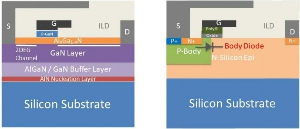
Figure 1: GaN HEMT (Enhancement-Mode) vs Silicon LDMOS Structure
From a structural perspective, both GaN power devices and Silicon LDMOS are lateral structures, meaning their source, gate, and drain are all located on the top surface of the chip. To ensure a more uniform electric field distribution, both technologies employ a field plate design. However, the main difference lies in the material composition and fabrication process.
GaN power devices utilize GaN compound semiconductor epitaxy to form a high electron mobility two-dimensional electron gas (2DEG) channel through heterostructures. On the other hand, Silicon LDMOS involves doping processes on a silicon epitaxial layer to form P-N junctions.
In summary, while both technologies have lateral structures with field plate designs for improved electric field distribution, GaN power devices rely on compound semiconductor epitaxy and heterostructures to create a high electron mobility channel, whereas Silicon LDMOS utilizes doping techniques on a silicon epitaxial layer to form P-N junctions.
2. The structure of GaN power devices
The epitaxial structure of GaN power devices can be divided into two types: D-mode (Depletion-mode) and E-mode (Enhancement-mode). Due to the polarization characteristics of the material, depletion-mode is the natural state of GaN power devices, while enhancement-mode can only be achieved by a special process that changes the threshold voltage from negative to positive.
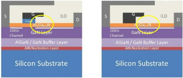
Figure 2: E-Mode (Enhancement-mode) GaN HEMT VS D-Mode (Depletion-mode) GaN HEMT
The current main approaches used to fabricate enhancement-mode devices include p-type gate, recessed gate, and F-treatment. As shown in the above figure, the P-GaN gate structure is one of the approaches to achieve enhancement-mode GaN HEMT. Essentially, it controls the gate voltage by reducing the electron density of the 2DEG (Two-Dimensional Electron Gas) beneath the gate, thereby increasing the threshold voltage to a positive value.
(1) D-Mode/Depletion-mode structure
D-Mode refers to normally-on devices, where in the typical state (gate-to-source voltage VGS = 0), there already exists a 2DEG between the drain and source, resulting in a conducting state of the device. When the gate-to-source voltage becomes VGS < 0, the 2DEG between the drain and source is cut off, resulting in device shutdown. In power electronics applications, normally-on devices are inconvenient to use and raise safety concerns. Therefore, D-Mode GaN HEMT devices are often used in conjunction with low-voltage silicon MOSFETs cascaded/connected in series, as shown in the figure below.
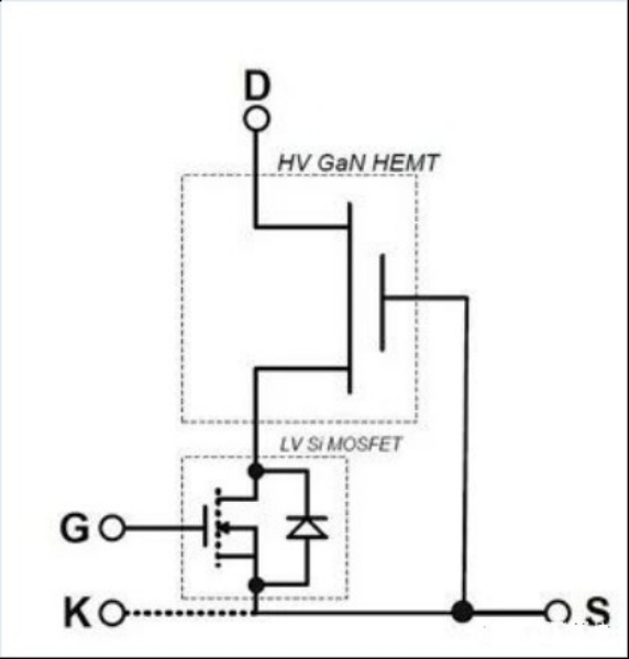
Figure 3: Common Source-Common Gate GaN HEMT
D-Mode GaN power devices are connected in series with low-voltage MOSFETs, sharing the gate and source to form normally-off devices.
(2) E-Mode/Enhancement-mode
E-Mode (Enhancement-mode) refers to normally-on devices. Its usage is similar to traditional silicon MOSFETs, with a simple device structure suitable for high-frequency applications. Enhancement-mode devices do not require negative voltage supply. In practical applications, GaN power devices are typically designed as normally-on devices.
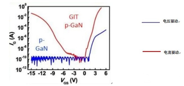
Currently, the mainstream enhancement-mode devices use P-GaN process structures, which lead to two technological approaches corresponding to two commercial models. One approach, represented by Panasonic and Infineon, is current-controlled. In this approach, the gate drive uses current rather than voltage for control. The other approach is similar to silicon MOSFETs and silicon carbide MOSFETs, using gate voltage drive.
To be continued...



Site Map | 萨科微 | 金航标 | Slkor | Kinghelm
RU | FR | DE | IT | ES | PT | JA | KO | AR | TR | TH | MS | VI | MG | FA | ZH-TW | HR | BG | SD| GD | SN | SM | PS | LB | KY | KU | HAW | CO | AM | UZ | TG | SU | ST | ML | KK | NY | ZU | YO | TE | TA | SO| PA| NE | MN | MI | LA | LO | KM | KN
| JW | IG | HMN | HA | EO | CEB | BS | BN | UR | HT | KA | EU | AZ | HY | YI |MK | IS | BE | CY | GA | SW | SV | AF | FA | TR | TH | MT | HU | GL | ET | NL | DA | CS | FI | EL | HI | NO | PL | RO | CA | TL | IW | LV | ID | LT | SR | SQ | SL | UK
Copyright ©2015-2025 Shenzhen Slkor Micro Semicon Co., Ltd