Service hotline
+86 0755-83044319

release time:2023-09-12Author source:SlkorBrowse:13371
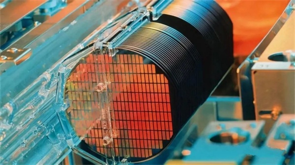
Plasma etching may be the most critical process in semiconductor manufacturing, and it can also be one of the most complex operations in all wafer fabrication processes, second only to lithography. Nearly half of the wafer manufacturing steps rely on plasma, a high-energy ionized gas, to perform their tasks.
Despite the continuous shrinking of transistors and storage units, engineers are still working on providing reliable etching processes.
Thomas Bondur, Vice President of Marketing for Lam Research's Etch Product Group, stated, 'In order to sustainably manufacture chips with nanometer-level precision and correct structures, equipment manufacturers for semiconductor fabs need to break through the boundaries of plasma physics, materials engineering, and data science to provide the required equipment solutions.' This is especially evident in plasma etching, which works hand in hand with lithography to create precise and repeatable features on wafers.
This report examines the key etching steps in 3D NAND, DRAM, nanosheet FET, and interconnects, and also looks ahead to 2D devices and backend processing. The industry is also pursuing more sustainable etching chemistries to reduce the equivalent carbon dioxide emissions from their wafer fabs.
For many tool manufacturers, process modeling plays a critical role in etch process development. The goal is to shorten time-to-market while reducing wafer and mask costs.
Barrett Finch, Senior Director of Marketing at Lam Research, said, 'Optimizing the etch process for some of the most challenging steps can take a year or more to complete. We recently completed some process simulations within three weeks, which were expected to take three months using typical silicon-based testing and development.'
In terms of mask and wafer costs alone, this can amount to hundreds of thousands or even millions of dollars for equipment manufacturers.
Etching Basics
Etching processes and lithography techniques work together in semiconductor manufacturing. Etching is typically performed before deposition of thin films (via epitaxy, chemical or physical vapor deposition, etc.). Generally, a CVD film is coated with a photoresist, and then optical lithography (248nm or 193nm UV, 13.5nm EUV) is used to expose the pattern through a photomask. The resist is then developed to reveal the pattern. In a single-wafer plasma etching chamber, etching chemicals and ion [敏感词]ardment are typically used to remove the CVD film with the photoresist mask as a guide (in positive-tone resists). After etching, the resist is ashed, followed by wet chemical cleaning and/or wet etching for residue removal.
Plasma etching processes can be roughly categorized into dielectric, silicon, or conductor etching. Dielectrics such as silicon dioxide and silicon nitride are best etched using fluorine-based gases, while silicon and metal layers react best with chlorine. There are basically three dry etching modes - reactive ion etching, plasma etching, and sputter etching (ion beam). Etching processes involve complex interactions between the reactive species, plasma, and chip materials. When an RF bias is applied to the reactive gas, electrons and positively charged ions physically remove (etch) material through [敏感词]ardment, while the chemical species and radicals react with exposed materials to form volatile by-products. Etching can be isotropic (equal vertical and lateral reaction rates), anisotropic (vertical only), or something in between.

Figure 1: The transition from finFET to GAA drives the critical need for isotropic selective etching. Source: Lam Research.
The key metrics that etching engineers are most concerned about are etch rate, profile control, uniformity (across the entire wafer), and etch selectivity, as these factors impact yield and productivity. Etch selectivity refers to the removal rate of the material being etched compared to its underlying layer, such as SiO2 on silicon. It is also advantageous to not remove excessive photoresist during the etching process. However, in such cases, it is typically transferred to a hard mask (silicon dioxide, silicon nitride, SiOC, TiN) before transferring the pattern onto the underlying film.
Selective specifications range from 2:1 to 1000:1 (highly selective etching). With each new node, these specifications become more stringent. Philippe Bézard, a dry etch R&D engineer at imec, said, "With high-NA EUV replacing conventional EUV within the next four years, the focus will be much lower, so you can no longer expose thick photoresists -- when I say thick, I mean 30 nanometers." "But you still need to pattern at the same film thickness underneath. So now you require higher selectivity because we have to achieve 10:1 instead of 2:1, which is a sudden increase in selectivity by 4 to 5 times.
To be continued...


Site Map | 萨科微 | 金航标 | Slkor | Kinghelm
RU | FR | DE | IT | ES | PT | JA | KO | AR | TR | TH | MS | VI | MG | FA | ZH-TW | HR | BG | SD| GD | SN | SM | PS | LB | KY | KU | HAW | CO | AM | UZ | TG | SU | ST | ML | KK | NY | ZU | YO | TE | TA | SO| PA| NE | MN | MI | LA | LO | KM | KN
| JW | IG | HMN | HA | EO | CEB | BS | BN | UR | HT | KA | EU | AZ | HY | YI |MK | IS | BE | CY | GA | SW | SV | AF | FA | TR | TH | MT | HU | GL | ET | NL | DA | CS | FI | EL | HI | NO | PL | RO | CA | TL | IW | LV | ID | LT | SR | SQ | SL | UK
Copyright ©2015-2025 Shenzhen Slkor Micro Semicon Co., Ltd
