Semiconductors have been a key industry of national development in recent years. So what exactly are semiconductors?
In daily life, all objects can be roughly classified by their electrical conductivity into three categories: conductors, semiconductors, and insulators.
This is easy to understand; objects either conduct electricity, do not conduct electricity, or conduct a little bit. It is precisely these materials that are ambiguous and exhibit partial conductivity that provide physicists with different opportunities for exploration.
Materials that are purely conductive or non-conductive are not very meaningful; it is the substances whose conductivity changes under different conditions that are interesting.
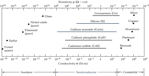
Let's take a look at the electrical conductivity of materials through a diagram for a more intuitive understanding.
According to their electrical conductivity:
Insulators: with a low electrical conductivity, approximately ranging from 20^-18S/cm to 10^-8S/cm, such as molten quartz and glass.
Conductors: with a higher electrical conductivity, ranging from 10^4S/cm to 10^6S/cm, such as metals like aluminum and silver.
Semiconductors: with electrical conductivity falling between that of insulators and conductors.
Common elemental semiconductors found in nature include silicon and germanium. It's said that germanium-based semiconductors were discovered and used even earlier than silicon-based ones, but the natural advantage of silicon is its affordability. Common sand in nature contains a large amount of silicon, you know!
Even though there is a lot of silica sand in nature, it contains too many impurities and defects, so it cannot be used directly and needs to be refined.
How do we refine it? In one word—burn!
Just like we learned in junior high school chemistry, we carry out oxidation-reduction reactions.
-
SiC + SiO2 → Si (solid) + SiO2 (gas) + CO (gas)
-
Si (solid) + 3HC → SiHCl3 (gas) + H2 (gas)
-
SiHCl3 (gas) + H2 (gas) → Si (solid) + 3HCl (gas)
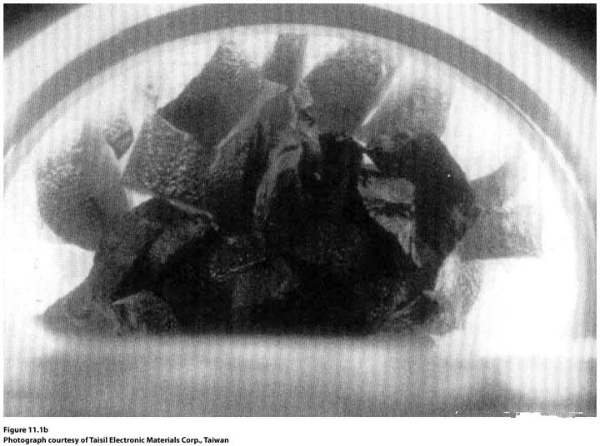
After three high-temperature chemical reactions, we obtain solid silicon, but at this point, the silicon is polycrystalline.
What is polycrystalline silicon?
Just like when we peel an orange, inside there are many segments (polycrystalline segments), and each segment tastes different (crystal orientation). We need to select the best-tasting segment and let it grow on its own!
How to make a small single crystal grow individually?
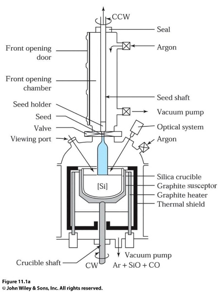
Physicists are indeed smart, inventing a method for growing single crystals called the Czochralski method, possibly named after the scientist who developed it.
There is also an intuitive industry term for this process, known as the Bridgman method!
Because when growing single crystals, it's like pulling the small crystals upwards! The pulling speed is a bit slow. Take a look at this device:
The blue cylindrical rod in the image is a single crystal silicon. During the pulling process, it rotates while being pulled upwards, resulting in a cylindrical ingot grown by the Bridgman method.
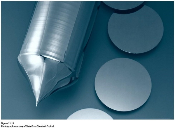
The grown ingot is then cut into disk-shaped pieces using mechanical blades, forming what we call wafers.
Does this process sound familiar to you?
That's how wafers are produced.
Although we now have the wafers, at this stage, the electrochemical properties of single crystal silicon are not sufficient for direct use in making chips. Engineers then work on modifying the electrochemical properties of single crystal silicon.
How do they modify single crystal silicon?
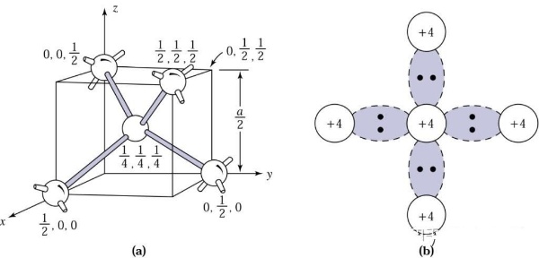
First, let's delve into some understanding of the silicon element. In the periodic table, silicon is positioned 14th. A silicon atom has four electrons in its outer shell, which it shares with four neighboring atoms, forming four pairs of shared electrons. This structure of shared electron pairs is known as covalent bonding. Each pair of electrons forms a covalent bond.
You may have learned about this part in middle school chemistry. Let's take a look at a picture for a more visual understanding:
The left image shows the crystal structure of single crystal silicon, which resembles the structure of a diamond crystal. On the right, we have a depiction of silicon atoms sharing electrons, with one silicon atom in the center sharing electrons with four "sibling" silicon atoms.
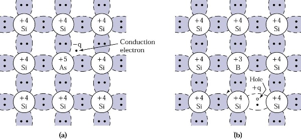
One day, a physicist had a sudden idea: What if silicon didn't share electrons with its "sibling" atoms and invited other "siblings" into the group?
One day, the physicist invited arsenic to join the group, and then a miracle happened:
The arsenic "sibling" has 5 electrons in its outer shell, with 4 electrons forming bonds with silicon atoms, leaving one electron unpaired. This unpaired electron becomes a free agent, wandering around and altering the conductivity of silicon due to its charge.
By providing an extra electron to the silicon family, the arsenic atom is known as a donor.
With the increase in free electrons in the silicon family, the negatively charged carriers increase, transforming silicon into an n-type semiconductor.
Why is it called "N-type"? In English, "Negative" represents negative. Taking the first letter of this word gives us N.
Similarly, the physicist thought, if we can introduce arsenic atoms with extra electrons, can we also invite boron atoms with fewer electrons into the group? So the physicist decided to bring boron atoms into the mix to see what happens.
Due to the boron atom having only 3 electrons in its outer shell, one fewer than silicon, each covalent bond that originally had 2 electron pairs now consists of just one pair, leaving behind a gap—a positively charged hole.
At this point, the silicon-based semiconductor is known as a p-type semiconductor. Similarly, "P" comes from the first letter of the English word "Positive," and the boron atom is referred to as an acceptor.
It is the introduction of different atoms into the single crystal silicon that results in the formation of N-type and P-type semiconductors.
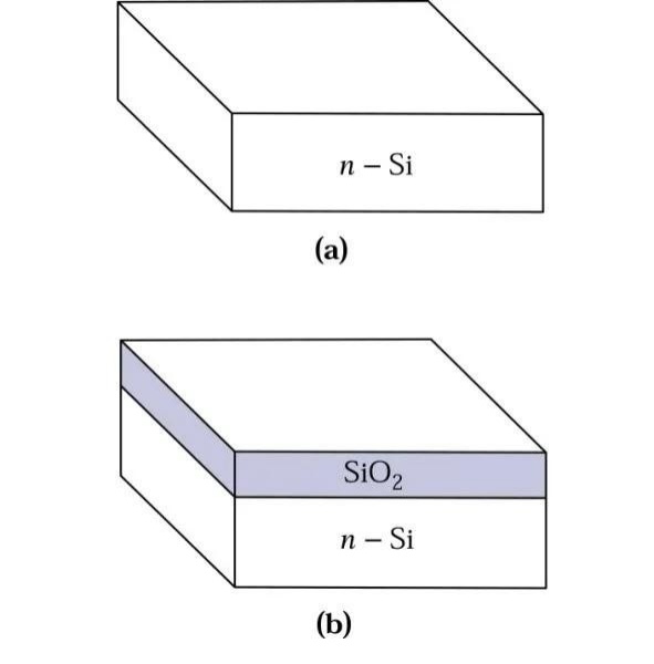
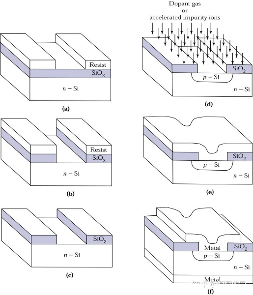
When we have single crystal silicon and can find a way to oxidize its surface into silicon dioxide, the silicon dioxide can serve as an insulator for many device structures or act as a barrier layer during device fabrication processes such as diffusion or ion implantation.
In the manufacturing process of a p-n junction, a thin layer of silicon dioxide can be used to define the region of the junction.
Take a look at this schematic diagram: (a) shows an uncovered silicon wafer, ready for the oxidation step, while (b) depicts only the top layer of the oxidized wafer.
With the theoretical knowledge of P-type and N-type semiconductors, we can take things a step further and modify the surface of silicon dioxide to create desired patterns, such as drawing a cat or a flower.
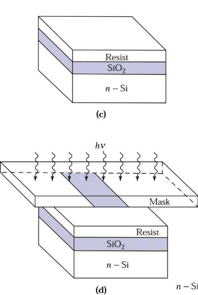
The method for modifying the wafer surface is called photolithography!
But doesn't photolithography require advanced equipment? I heard those machines are really impressive... Let's first understand the principle of photolithography:
Using a high-speed spin coater, a layer of ultraviolet (UV) light-sensitive material called photoresist is spun onto the surface of the chip. After removing the chip from the spinner, it is baked at a temperature between 80°C and 100°C to drive off the solvent in the photoresist and harden it, enhancing its adhesion to the chip.
Next, a UV light source is used to expose the chip through a patterned mask. Then, buffered hydrofluoric acid is used as an acid etchant to remove the unprotected silicon dioxide surface. Finally, the photoresist is stripped using a chemical solvent or a plasma ashing system.
Take a look at the schematic diagram: Only (a) is shown.
The process is somewhat akin to making a seal. First, a model is painted on a stone with pigment, then it is carved according to the model's dimensions. It's essentially the same principle.
Just like seals can have raised or recessed designs, wafers can also be treated similarly. Depending on the choice of photoresist, either positive or negative, one can achieve raised (positive) and recessed (negative) patterns. The photoresists used are referred to as positive resist and negative resist.
After photolithography, the silicon surface is exposed to the outside environment. Physicists then introduce other elements into this silicon surface through a process known as ion implantation.
When boron (B) or arsenic (As) ions are implanted, they alter the traditional properties of silicon, changing its electrochemical characteristics. At this point, the semiconductor is termed an extrinsic semiconductor.
The junction formed by the contact between P-type and N-type semiconductors is called a p-n junction!
After doping is completed, efforts are made to extract the performance of this semiconductor. This involves metallizing the semiconductor surface, with steps including ohmic contact and interconnect completed in the subsequent metallization process. Metal thin films can be formed using physical vapor deposition (PVD) or chemical vapor deposition (CVD).
With the completion of metallization, the p-n junction can now function!
That's all for the basic semiconductor knowledge!