The bipolar junction transistor was invented by a research team at Bell Laboratories in 1947. The first transistor consisted of two metal wires with sharp endpoints making point contact with a germanium substrate. While primitive by today's standards, this first transistor significantly transformed the entire electronics industry and the way of life for humanity.
In modern bipolar junction transistors, silicon has replaced germanium as the substrate, and point contact has been replaced by two adjacent coupled p-n junctions. The structure can take the form of p-n-p or n-p-n.
A transistor, short for "transfer resistor," is a multi-junction semiconductor device. Typically integrated with other circuit components, transistors are used to achieve voltage, current, or signal power amplification.
Bipolar transistors, also known as bipolar junction transistors (BJTs), are among the most important semiconductor devices and find wide applications in high-speed circuits, analog circuits, power amplification, and more.
What is a P-N Junction?
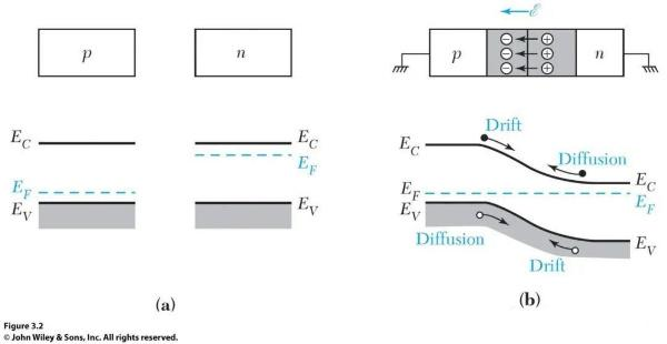
It is a junction formed by the contact between a p-type semiconductor and an n-type semiconductor.
For example, a p-type semiconductor is like a square piece of clay filled with many holes (known as electron holes), similar to the burrows seen in lobsters. An n-type semiconductor is also a square piece of clay, but it is filled with many lobsters (free electrons). When we stick these two pieces of clay together, the lobsters will crawl towards the burrows.
The frontmost lobsters are the first to find the burrows in the front row. Once the front row lobsters have crawled into the burrows, the lobsters behind them have to climb farther and face greater difficulty in finding burrows.
As the burrows in the front rows are already nearly depleted, the semiconductor industry refers to this area as the depletion region.
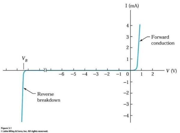
The P-N junction has a characteristic called rectification, which allows current to flow in only one direction.
It's like a door: it's easy for a person to push the door open in one direction, but it's hard if you try to push it in the opposite direction. Of course, you can use a great force to violently push the door until it breaks, a process we refer to as breakdown of the junction.
Looking at the current-voltage characteristics of a P-N junction, the curve is as shown in the diagram below.
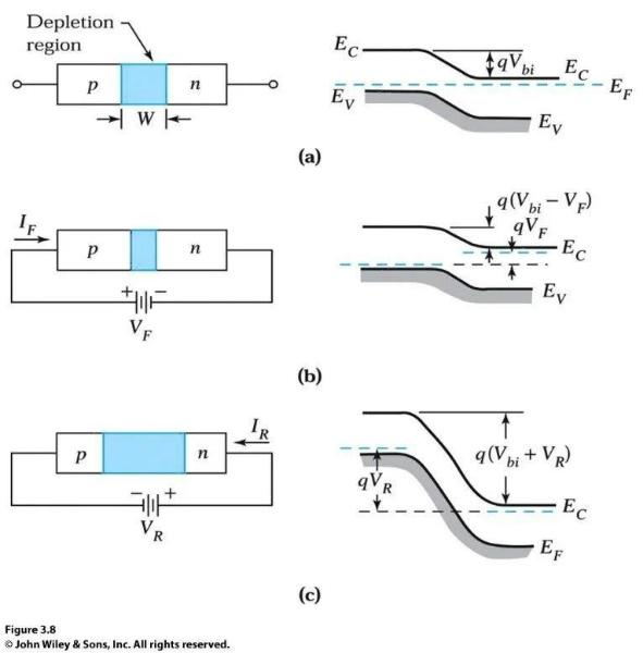
When a forward bias is applied to a P-N junction, it's like putting blindfolds on the lobsters in the mud. The lobsters become shortsighted and can only see the burrows in the front row. As a result, the overall movement of the lobsters decreases, and the number of lobsters crawling towards the burrows also decreases, reducing the width of the depletion region.
When a reverse bias is applied to a P-N junction, it's like giving the lobsters telescopes in the mud. The lobsters can see farther and crawl more excitedly, leading to more lobsters finding burrows. Consequently, the overall movement of the lobsters increases, and the width of the semiconductor's depletion region expands.
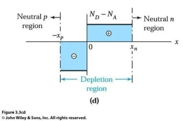
In the figure below, (a) represents the normal width of the depletion region in a P-N junction, (b) shows the width after applying a forward bias, and (c) shows the width after applying a reverse bias.
The structure of a bipolar transistor:
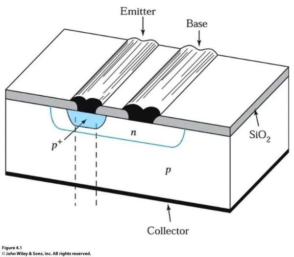
The diagram below shows a perspective view of a p-n-p bipolar transistor. The manufacturing process involves using a p-type semiconductor as the substrate, utilizing the principle of thermal diffusion to create an n-type region on the p-type substrate. Subsequently, a high concentration p+ type region is formed on this n-type region through thermal diffusion. Finally, metal is used to cover the p+, n, and underlying p-type regions to form ohmic contacts.
The p-n-p bipolar transistor consists of three regions with different doping concentrations, forming two p-n junctions. The highest concentration p+ region is called the emitter (denoted by E);
The intermediate narrow n-type region, with a moderate impurity concentration, is called the base (denoted by B), and the width of the base region needs to be much smaller than the diffusion length of minority carriers;
The region with the lowest concentration of p-type is called the collector (denoted by C). Assuming uniform distribution of concentrations within each region, the concept of the p-n junction can be directly applied to the junctions within the transistor.
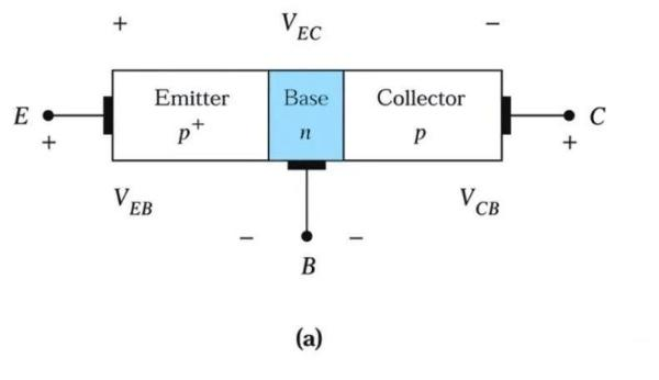
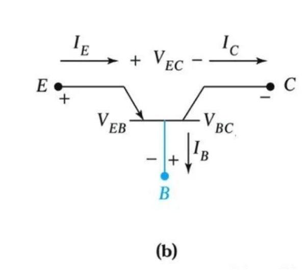
The diagram below shows the circuit symbol of a p-n-p bipolar transistor, indicating the various current components and voltage polarities. The arrows and "+" and "–" symbols represent the directions of the currents and the polarities of the voltages in the general working mode (i.e., amplification mode, active mode) of the transistor. In this mode, the emitter-base junction is forward biased (VEB > 0), while the collector-base junction is reverse biased (VCB < 0). According to
Kirchhoff's circuit law, for this three-terminal device, there are only two independent currents; if any two currents are known, the third terminal current can be determined.
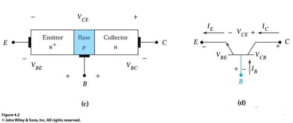
The structure and circuit symbol of an n-p-n bipolar transistor are complementary to those of a p-n-p bipolar transistor. The diagram below shows the ideal structure and circuit symbol of a p-n-p transistor.
Replacing the p-type regions with n-type regions and the n-type region with a p-type region in the structure of a p-n-p bipolar transistor yields the structure of an n-p-n bipolar transistor. Therefore, the current direction and voltage polarity are also reversed.
Understanding the p-n-p transistor, one can describe the n-p-n transistor by simply swapping the polarity and doping types.
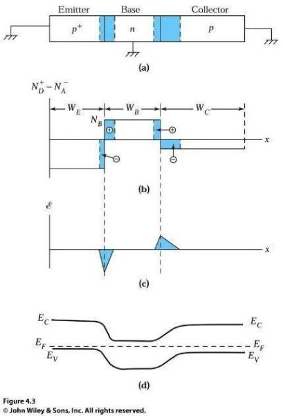
The diagram (a) shows the ideal p-n-p bipolar transistor in thermal equilibrium, where its three terminals are connected together or all connected to ground, with shaded regions representing the depletion regions of the two p-n junctions.
Diagram (b) illustrates the impurity concentrations in the three doped regions, with the emitter region having a much higher doping concentration than the collector region, and the base region having a concentration lower than the emitter but higher than the collector.
Diagram (c) depicts the electric field distribution in the depletion region.
Diagram (d) displays the energy band diagram of the transistor, extending the thermal equilibrium state of the p-n junctions and applying it to the two adjacent coupled p+ - n junctions and n - p junction.
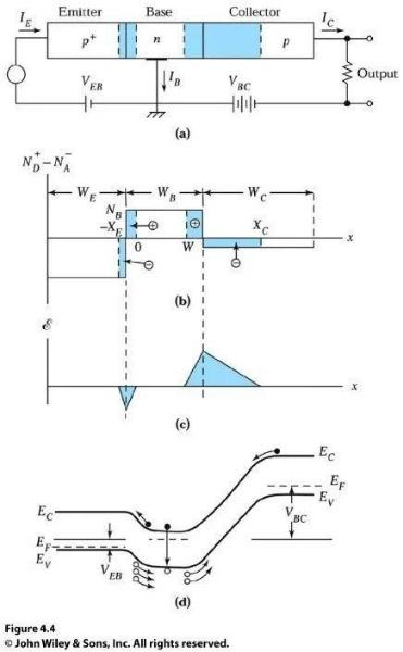
The following diagram corresponds to the transistor operating in the amplification mode as depicted in the previous illustration.
Diagram (a) shows the transistor connected as a common-base configuration amplifier, where the base is shared between the input and output circuits.
Diagrams (b) and (c) illustrate the charge density and electric field distribution under bias conditions, compared to the thermal equilibrium state depicted in the previous diagram. The width of the depletion region at the emitter-base junction narrows, while the depletion region at the collector-base junction widens.
Diagram (d) displays the energy band diagram of the transistor operating in amplification mode. The emitter-base junction is forward biased, causing holes to be injected from the p+ emitter region into the base region, and electrons to be injected from the base region into the emitter region.
In an ideal diode, there is no generation-recombination current in the depletion region, so the holes injected from the emitter region to the base region and the electrons injected from the base region to the emitter region constitute the emitter current.
On the other hand, the collector-base junction is reverse-biased, allowing a reverse saturation current to flow. If the base region is narrow enough, the holes injected from the emitter region into the base region can diffuse through the base region and reach the edge of the collector-base depletion region, eventually flowing through the collector region under the biasing of the collector-base junction.
This transport mechanism gives rise to the names "emitter" for injecting charge carriers and "collector" for collecting carriers injected from the adjacent junction.
If most of the injected holes do not recombine with electrons in the base region but reach the collector, the collector current due to holes will closely match the emitter hole current.
It is evident that the holes injected from the adjacent emitter-base junction can generate a significant current in the reverse-biased collector-base junction, leading to the amplification effect of the transistor, which occurs only when these two junctions are sufficiently close together, hence referred to as interacting p-n junctions.
Conversely, if these two p-n junctions are too far apart, all incoming holes will recombine with electrons in the base region and not reach the collector region, resulting in no amplification effect of the transistor. In this case, the p-n-p structure simply acts as two back-to-back connected p-n diodes.
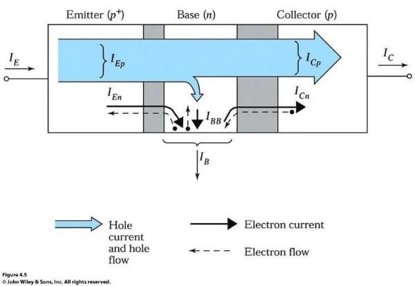
Current gain: The diagram below illustrates the various current components in an ideal p-n-p transistor operating in the amplification mode. Assuming no generation-recombination current in the depletion region, the holes injected from the emitter region constitute the predominant current component IEp.
Most of the incident holes will reach the collector electrode and form ICp.
There are three currents at the base: IBB, IEn, and ICn.
IBB represents the current of electrons supplied by the base that recombine with the incident holes (i.e., IBB = IEp - ICp); IEn represents the current of electrons injected from the base region into the emitter region, which is an undesirable current component that can be reduced by heavy doping of the emitter or using heterojunctions; ICn represents the electron current generated near the collector junction due to thermal effects, flowing from the collector region to the base region.
Operating modes: Depending on the bias voltages on the emitter-base junction and collector-base junction, bipolar transistors have four operating modes.
The diagram below illustrates the four operating modes of a p-n-p transistor and their relationships with VEB and VCB. The distribution of minority carriers in each operating mode is also shown in the diagram.
For example, in the amplification mode, the emitter-base junction is forward biased, and the collector-base junction is reverse biased.
In the saturation mode, both junctions of the transistor are forward biased, leading to the presence of minority carriers in the depletion regions of both junctions.
In saturation mode, a small voltage can result in a large output current, putting the transistor in a conducting state similar to a short circuit.
In the cutoff mode, both junctions of the transistor are reverse biased, leading to boundary conditions of pn(0) = pn(W) = 0. The transistor in cutoff mode can be seen as a switch in the open (or off) position.
In the inverted mode, the emitter-base junction is reverse biased, and the collector-base junction is forward biased. In this mode, the collector electrode functions as the emitter and vice versa. However, the current gain in the inverted mode is typically smaller than in the amplification mode due to the lower doping concentration in the collector region compared to the base region, resulting in lower "emission efficiency."
Switching transient process: In digital circuits, transistors mainly act as switches. By using a small base current, the collector current can be quickly changed from off to on (and vice versa) in a very short time. In the off state, there is high voltage and low current, while in the on state, there is low voltage and high current.
Heterojunction Bipolar Transistors (HBTs) refer to transistors where one or both junctions are made of different semiconductor materials.
The main advantage of HBTs is their high emission efficiency, and they are used similarly to bipolar transistors. However, HBTs have higher speed and can operate at higher frequencies. Due to these characteristics, HBTs are widely used in optoelectronics, microwave, and digital applications. In microwave applications, HBTs are commonly used to manufacture solid-state microwave and millimeter-wave power amplifiers, oscillators, and mixers.
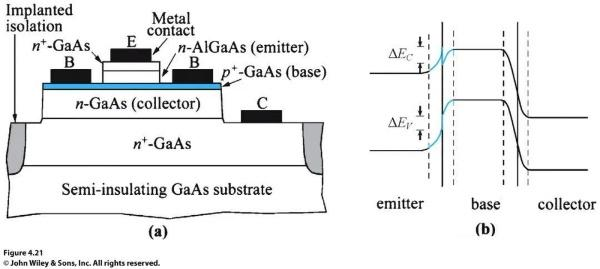
Basic HBT structure: Most HBT technologies are developed in the AlxGa1-xAs/GaAs material system. The basic n-p-n HBT structure consists of a wide bandgap AlxGa1-xAs layer in the n-type emitter region, a narrower bandgap GaAs layer in the p-type base region, and n-type collector and subcollector regions made of lightly doped and heavily doped GaAs, respectively.
To form an ohmic contact, a highly doped n-type gallium arsenide layer is added between the emitter contact and the aluminum gallium arsenide layer. Due to the significant difference in bandgap width between the emitter and base regions, the common-emitter current gain can be increased significantly. In contrast, homojunction bipolar transistors do not have such a bandgap width difference, and thus, the doping concentration ratio between the emitter and base regions must be increased significantly. This fundamental difference sets apart homojunction from heterojunction bipolar transistors.
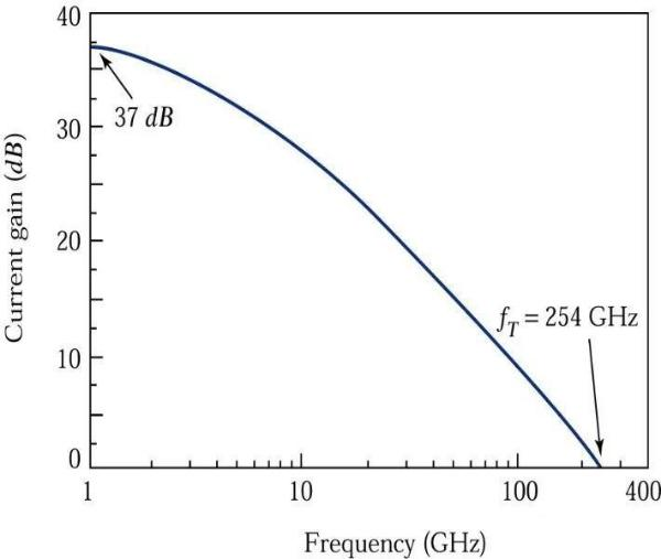
Advanced HBTs: In recent years, materials from the InP series (such as InP/InGaAs or AlInAs/InGaAs) have been systematically researched, and InP-based heterostructures offer numerous advantages. The InP/InGaAs structure exhibits extremely low surface recombination, and the electron mobility of InGaAs is much higher than that of GaAs, resulting in excellent high-frequency performance.
The graph below depicts the characteristic curve of a typical indium phosphide-based HBT, with a cutoff frequency reaching up to 254 GHz. Additionally, InP demonstrates a higher drift velocity than GaAs under strong electric fields and also has a higher breakdown voltage.
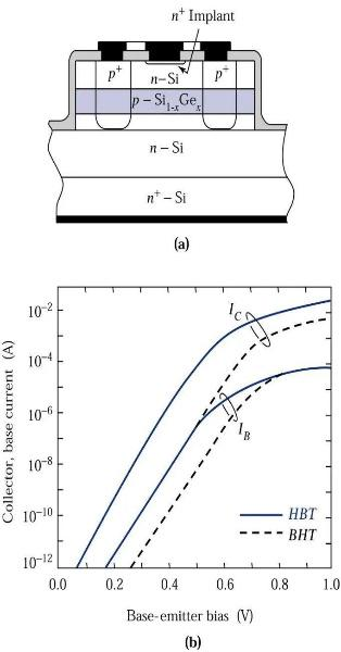
Another type of heterojunction is the Si/SiGe material system, which offers several attractive features for HBT applications. Similar to the AlGaAs/GaAs HBT, the Si/SiGe HBT also benefits from the ability to heavily dope due to the bandgap width difference, resulting in high-speed performance.
The low density of silicon interface traps helps reduce surface recombination current, ensuring high current gain even at low collector currents. Additionally, compatibility with standard silicon processing technology is another highly attractive feature.
The diagram in (a) illustrates a typical Si/SiGe HBT structure, while (b) compares the collector current of the Si/SiGe HBT with that of a silicon homojunction bipolar transistor, showing that the Si/SiGe HBT exhibits higher current gain. Compared to gallium arsenide and indium phosphide-based HBTs, the Si/SiGe
HBT has a lower cutoff frequency due to the lower carrier mobility of silicon.
Section VI: Thyristor Devices and Related Power Devices
Thyristor devices are crucial power components capable of controlling high voltage and high current, enabling the device to transition from a closed or blocked state to an open or conducting state, and vice versa. Their operation is closely related to bipolar transistors, involving the conduction of both electrons and holes.
However, their switching mechanism and structure differ from bipolar transistors, offering a wide range of current and voltage control capabilities. The rated current can range from a few milliamperes to over 5000A, with a rated voltage exceeding 10,000V.
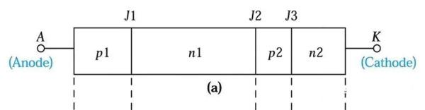
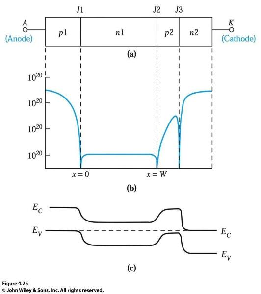
Basic Characteristics: The diagram below illustrates the cross-section of a thyristor device, which consists of a four-layer p-n-p-n structure formed by three series-connected p-n junctions, namely J1, J2, and J3. The outermost p-layer connected to the contact electrode is called the anode, while the other side's n-layer is referred to as the cathode. This structure, without additional electrodes, represents a two-terminal device and is known as a p-n-p-n diode.
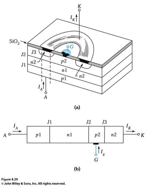
If another electrode, known as the gate, is connected to the inner p2 layer, the resulting three-terminal device is called a semiconductor-controlled rectifier (SCR) or thyristor.
The diagram in (b) shows a typical doping profile of a thyristor device. It begins with a high-resistivity n-type silicon wafer as the starting material (n-layer), followed by a diffusion step to simultaneously form the p1 and p2 layers. Lastly, alloying or diffusion is used to create the n2 layer on one side of the silicon wafer.
Diagram (c) illustrates the energy band diagram of the thyristor device in thermal equilibrium. Each junction has a depletion layer, and the built-in potential is determined by the doping concentration.
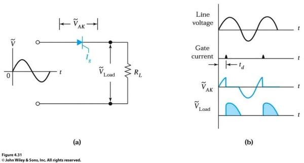
The diagram illustrates a simple application of a thyristor device, which can adjust the power delivered from the power line to the load. The load, RL, could be a light bulb or a heater, for example. The power delivered to the load in each cycle is controlled by the gate current pulse of the thyristor device.
If the gate current pulse is applied close to the beginning of each cycle, more power will be transferred to the load. Conversely, delaying the gate current pulse will result in significantly reduced power being delivered to the load as the thyristor device conducts towards the end of the cycle.
This is all the information regarding bipolar transistors.