Service hotline
+86 0755-83044319

release time:2024-01-31Author source:SlkorBrowse:16000
Introduction
Intel is a global leader in the semiconductor industry and innovation, dedicated to driving innovation and breakthroughs in technologies such as artificial intelligence, 5G, and high-performance computing, and powering the intelligent interconnected world. 56 years ago, one of Intel's founders, Gordon Moore, proposed Moore's Law, which has been driving the development of the integrated circuit industry to this day. In the field of advanced packaging, Intel remains a technological leader, creatively introducing advanced packaging and interconnect technologies such as EMIB, Foveros, Co-EMIB, and ODI, continuing to drive technology forward. Today, we have the opportunity to connect with Johanna Swan, Director of Packaging Research and System Solutions at Intel, to engage in in-depth communication and exchange about advanced packaging technology, and to learn about the cutting-edge developments in advanced packaging. In the personal computer field, Intel is undoubtedly the most creative company. Intel Inside has deeply penetrated people's hearts. From Pentium to Core, and then to i3, i5, i7, and i9, each product brings people a brand-new experience, driving the digital world forward continuously.
The era of heterogeneity has arrived. Has Intel unleashed new creativity, and what new technologies and products will it bring to the world? Let's listen to the voice from Intel.
Suny Li
First, we would like to ask Director Swan to talk about Intel's research and development plan and the latest research results in the field of advanced packaging technology.
Johanna Swan
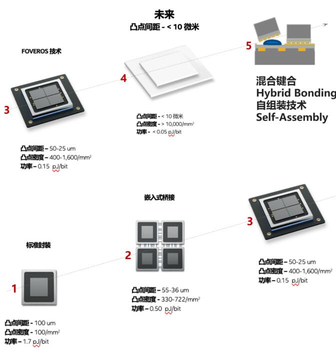
Sure, first I'd like to share with everyone Intel's roadmap for advanced packaging technology. The X-axis in the chart represents power efficiency, the Y-axis represents interconnect density, and the Z-axis demonstrates the scalability of our technology.
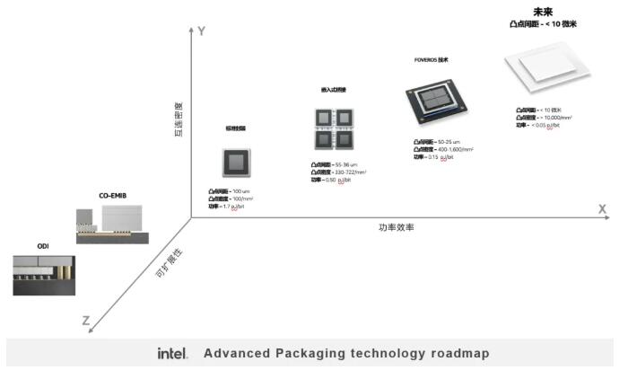
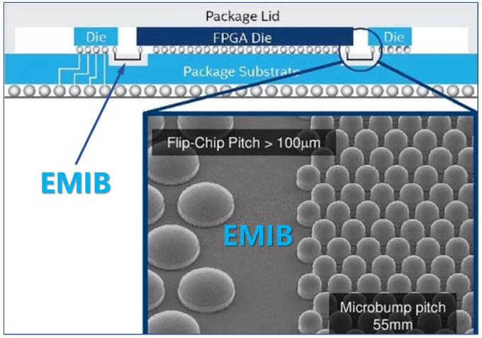
From standard packaging to embedded multi-chip interconnect bridge (EMIB), more chips are being included in the package, and the pitch between bumps is becoming smaller, decreasing from 100um to 55-36um.
Next, Intel aims to achieve bump pitches smaller than 10um. What does achieving a bump pitch smaller than 10 micrometers mean? This brings us to Intel's Hybrid Bonding technology.
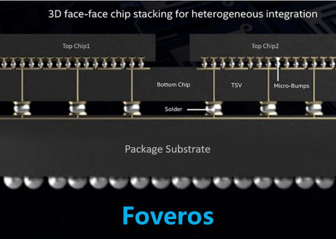
At this year's ECTC, Intel presented a paper on Hybrid Bonding technology, which is a method to achieve denser interconnects between stacked chips and enables smaller form factors. The technology on the left side of the diagram, known as Foveros, has a bump pitch of 50 micrometers, with approximately 400 bumps per square millimeter. For the future, Intel aims to reduce the bump pitch to approximately 10 micrometers and achieve 10,000 bumps per square millimeter.
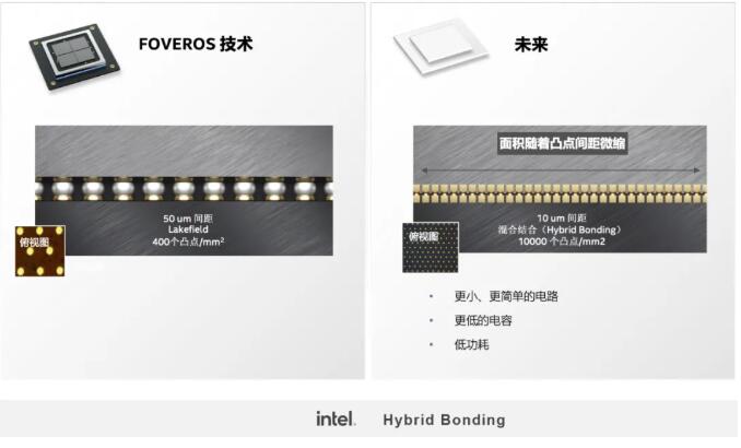
Hybrid Bonding technology enables more interconnects between chips, resulting in lower capacitance, reduced power per channel, and a direction towards delivering superior products.
The following diagram compares traditional bump bonding technology with Hybrid Bonding technology. Hybrid Bonding technology requires new manufacturing, handling, cleaning, and testing methods. The advantages of Hybrid Bonding technology include higher current carrying capacity, scalable pitches below 1 micron, and improved thermal performance.
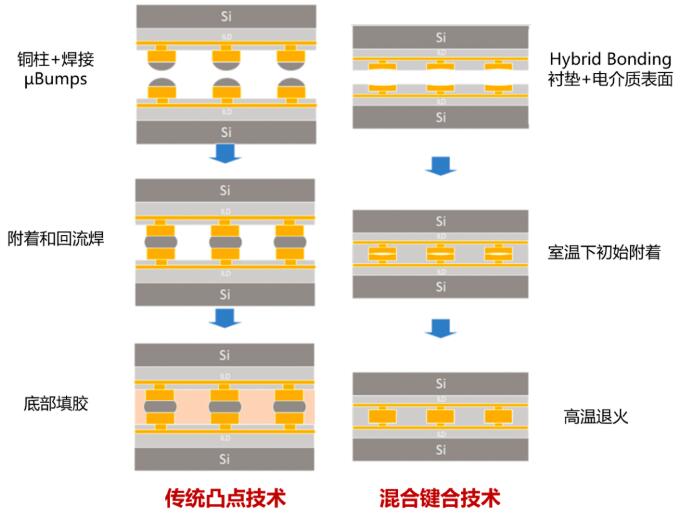
From the diagram, we can see that in traditional bump bonding technology, there are copper pillars with solder between the two chips. They are attached together through reflow soldering and then filled with underfill.
Hybrid Bonding technology, on the other hand, is different from traditional bump bonding. It does not have prominent bumps. The specially manufactured dielectric surface is very smooth, in fact, it even has a slight recess. The two chips are attached together at room temperature, and then elevated in temperature for annealing. At this point, copper expands and firmly bonds together, forming an electrical connection.
Hybrid Bonding technology allows for a reduction in interconnect pitch to below 10 micrometers, achieving higher current carrying capacity, denser copper interconnect density, and better thermal performance compared to underfill. Of course, Hybrid Bonding technology requires new manufacturing, cleaning, and testing methods.
Now, why is a smaller pitch more attractive? Intel is shifting towards a chiplet design approach, where SoCs are decomposed into GPU, CPU, IO chips, which are then integrated within a single package using SiP technology. Additionally, through chiplet technology, smaller blocks have individual IPs and can be reused. This is an excellent technique that allows for customized products based on specific customer needs.
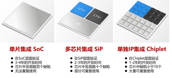
Chiplet technology has revolutionized chip-to-chip interconnects, as more chip-to-chip connections require higher interconnect density. This has led to a shift from traditional bump bonding to hybrid bonding.
Furthermore, we face another challenge in how to assemble these chips together while maintaining the manufacturing process at the same speed. With more chips to place, can we process them fast enough by placing only one chip at a time? The solution lies in batch assembly, which we refer to as self-assembly technology.
Intel is actively collaborating with CEA-LETI, the French Alternative Energies and Atomic Energy Commission's Laboratory for Electronics & Information Technology, to research the placement of multiple chips in a single process step. This involves deterministic and rapid placement, as well as picking and placing more chips.
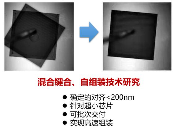
During the self-assembly process, chips have the ability to restore themselves to their lowest energy state. By bringing them close enough, they will autonomously assemble and position themselves in the minimum energy configuration. This is a self-assembly mechanism being researched by Intel in collaboration with CEA-LETI.
We have already incorporated hybrid bonding and self-assembly technologies into our roadmap for advanced packaging technology.


Site Map | 萨科微 | 金航标 | Slkor | Kinghelm
RU | FR | DE | IT | ES | PT | JA | KO | AR | TR | TH | MS | VI | MG | FA | ZH-TW | HR | BG | SD| GD | SN | SM | PS | LB | KY | KU | HAW | CO | AM | UZ | TG | SU | ST | ML | KK | NY | ZU | YO | TE | TA | SO| PA| NE | MN | MI | LA | LO | KM | KN
| JW | IG | HMN | HA | EO | CEB | BS | BN | UR | HT | KA | EU | AZ | HY | YI |MK | IS | BE | CY | GA | SW | SV | AF | FA | TR | TH | MT | HU | GL | ET | NL | DA | CS | FI | EL | HI | NO | PL | RO | CA | TL | IW | LV | ID | LT | SR | SQ | SL | UK
Copyright ©2015-2025 Shenzhen Slkor Micro Semicon Co., Ltd
