Service hotline
+86 0755-83044319

release time:2023-10-14Author source:SlkorBrowse:12577
2.5 EUV as an Analytical Tool
At the working group meeting, researchers from NIST discussed three main themes related to using EUV as an analytical tool to assist the semiconductor manufacturing industry. The three methods for utilizing EUV light as an analytical technique are: (1) high harmonic generation (HHG), (2) synchrotron radiation, and (3) atomic probe tomography. High harmonic generation offers a compact footprint, allowing deployment in research and manufacturing facilities with continuous access to dimensions, materials, and dynamic characteristics of deep sub-nanometer-level microelectronic devices, which are typically studied using synchrotron radiation sources. Synchrotron radiation sources allow studying various aspects of EUVL and provide additional capabilities to study the degradation of collector mirrors. Atomic probe tomography is the only technique that can provide 3D chemical mapping on the atomic level with sub-nanometer isotopic resolution for any element on the periodic table, which can be used for the study of EUV photoresists.
The industry has provided valuable feedback on the potential uses of these tools in assisting EUVL manufacturing. The NIST legal committee must take proactive action to develop solutions to meet potential collaborators' requests for Non-Disclosure Agreements (NDAs) while fulfilling the unique legal and administrative requirements arising from federal employment, explicitly prohibiting themselves or their organization from complying with any external contracts.
2.5.1 High Harmonic Generation (HHG)
As EUVL pushes lithography further into the deep sub-nanometer scale regime, the microelectronics industry is calling for new measurement and metrology techniques. At NIST, there is an ongoing project utilizing EUV's short wavelength to probe dimensions, materials, and dynamic characteristics of microelectronic devices at the deep sub-nanometer scale. NIST's high harmonic generation (HHG) light source is a broadband (spanning 20-100 eV photon energies), ultrafast (20 femtosecond pulses), and coherent (laser-like) source. The broad spectral coverage allows access to core-level transitions in many relevant materials for measurements of microelectronic devices and specific layers, as shown in Figure 13. Such measurements are typically performed using synchrotron radiation sources. However, the compact footprint of HHG sources allows for deployment in research and manufacturing facilities with continuous access. Figure 14 shows a photograph of the current system operating at the NIST Physical Measurement Laboratory (PML), which fits within typical laboratory space.
.png")
Figure 13 shows the photon energy output spectrum of the NIST high harmonic generation (HHG) source and the positions of several atomic core level transitions in relevant materials.
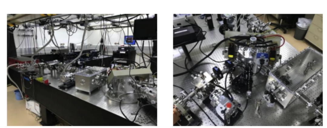
Figure 14. Photograph of the HHG source located at NIST and the accompanying instrumentation.
The short pulse width enables dynamic measurements of spin and thermal transport. One recent success is the development of a frequency comb generator synchronized with EUV pulses, with jitter better than two picoseconds. Figure 15 demonstrates this synchronization with a 40 GHz signal. This is an improvement of approximately one order of magnitude compared to what can be achieved on a synchrotron accelerator, allowing us to perform measurements at the operating frequencies of microelectronic devices. This enables real-time measurements of heat flow and spin transport inside and outside functional devices.
.png")
Figure 15. 40 GHz signal on the sampling oscilloscope. The triggering pulse (in red) is derived from the pulses used in the high harmonic generation system, directly demonstrating the synchronization between the high harmonics and the 40 GHz signal.
Finally, the coherence of light enables lensless imaging techniques such as coherent diffraction imaging, ptychography, and holography, which can provide spatial resolution at EUV wavelengths. This capability allows NIST to directly image functional devices, although this work has not been completed at NIST. Figure 16 shows the result of combining ptychography with reflectometry to measure the lateral spatial distribution of dopants in silicon. This approach enables non-destructive evaluation of interfaces and dopant distributions in microelectronics.
.png")
Figure 16. Example of 3D nanoscale characterization of dopant distribution using a combination of reflectometry and ptychography. Source: Tanksalvala.
At the working group meeting, industry representatives mentioned how analyzing semiconductor components on wafers to identify defects can be useful. Specifically, Golani et al. demonstrated how separating simulation of light-structure interactions from optical simulation in a systematic simulation allowed for testing of many optical configurations in a relatively short amount of time during post-processing. The Golani et al. simulation was performed using the Ansys commercial solver and featured a powerful digital twin.
To be continued...


Site Map | 萨科微 | 金航标 | Slkor | Kinghelm
RU | FR | DE | IT | ES | PT | JA | KO | AR | TR | TH | MS | VI | MG | FA | ZH-TW | HR | BG | SD| GD | SN | SM | PS | LB | KY | KU | HAW | CO | AM | UZ | TG | SU | ST | ML | KK | NY | ZU | YO | TE | TA | SO| PA| NE | MN | MI | LA | LO | KM | KN
| JW | IG | HMN | HA | EO | CEB | BS | BN | UR | HT | KA | EU | AZ | HY | YI |MK | IS | BE | CY | GA | SW | SV | AF | FA | TR | TH | MT | HU | GL | ET | NL | DA | CS | FI | EL | HI | NO | PL | RO | CA | TL | IW | LV | ID | LT | SR | SQ | SL | UK
Copyright ©2015-2025 Shenzhen Slkor Micro Semicon Co., Ltd
